
QPHY-DDR2
The LeCroy QPHY-DDR2 Test Solution is the best way to characterize DDR2 memory interfaces. Capable of performing measurements on 400 MHz, 533 MHz, 667 MHz, 800 MHz, 1066 MHz and custom speed grades, QPHY-DDR2 has a full suite of Clock, Electrical and Timing tests as specified by the JEDEC Specification and Intel JEDEC Specifications Addendums.
Key Features
- Support for testing 400 MHz, 533 MHz, 667 MHz, 800 MHz, 1066 MHz and custom speed grades of DDR2 signals
- Fastest way to gain confidence in your DDR2 interface by measuring a large number of cycles and reporting statistical results
- Fully annotated worst case measure ment screenshot captured and displayed in report including trace labels and pertinent voltage levels
- Stop on test/failure capability allows the user to pause at a particular test and review the measure on the oscilloscope display
- Complete test coverage for tests as described by the JESD79-2E and JESD208 JEDEC Specifications and Intel DDR2 667/800 JEDEC Specifications Addendum Rev. 1.1 and Intel DDR2 400/ 533 JEDEC Specifications Addendum Rev. 1.0
The LeCroy QPHY-DDR2 Test Solution is the best way to characterize DDR2 memory interfaces. Capable of performing measurements on 400 MHz, 533 MHz, 667 MHz, 800 MHz, 1066 MHz and custom speed grades, QPHY-DDR2 has a full suite of Clock, Electrical and Timing tests as specified by the JEDEC Specification and Intel JEDEC Specifications Addendums.
The LeCroy QualiPHY platform provides an easy to configure user interface, allows for custom test and limit selection, displays connection diagrams to the user to ensure proper connectivity, and generates reports with all of the results including screenshots of the worst case failures for each applicable test. In addition, all of the waveforms tested by QPHY-DDR2 can be saved to easily share information or rerun the tests at a later time.
QPHY-DDR2 enables the user to obtain the highest level of confidence in their DDR2 interface. Due to the high level of variability in DDR2 measurements it is important to measure a large number of cycles. By measuring a large number of cycles in a very short period of time the user can be more confident that they are catching the true maximum and minimum points for their measurement.
In addition to automated characterization of DDR2 signals, QPHY-DDR2 also enables powerful debug capability for DDR2 signals inside the oscilloscope. Root causes of failure can be quickly and easily found using all of the advanced serial data tools within the oscilloscope. These include: SDA II, Eye Doctor? II, WaveScan?, and many more.
Clock Tests?– These tests perform all of the clock test as described by the appropriate JEDEC specification. These include average clock period, absolute clock period, average high/low pulse width, absolute high/low pulse width, half period jitter, clock period jitter, cycle-to-cycle period jitter and cumulative error over n period tests.
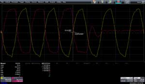
Electrical Tests?– These tests measure the electrical characteristics of the DDR2 signals. Shown above, the SoutR test measures the slew rates of the data, strobe and clock signals. Over 1000 slew rate measurements were performed and the worst instance was displayed on the screen. The signals are annotated with the signal names to make the screen easy to interpret. Additionally, cursors are used to show the user the voltage levels between which the slew rate was measured.
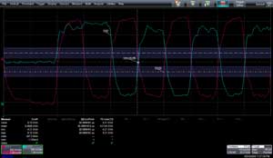
Timing Test?– These tests verify the timing relationship between particular DDR2 events. Shown above, the tDQSCK test verifies that the strobe output access time from the clock signal is within the limit specified by the appropriate JEDEC specification. In this test, 5000 tDQSCK measurements were performed on all of the DDR2 read bursts and the worst instance was displayed on the screen.
Eye Diagrams?– Eye Diagrams are a powerful tool for debugging serial data signals. QPHY-DDR2 enables the user to create eye diagrams of both the Read and the Write data bursts to ensure that the signal integrity is sufficient such that the data will be sampled properly by the receiver.

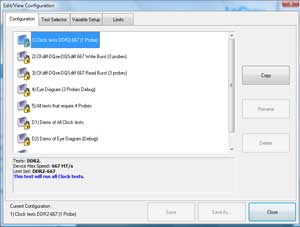
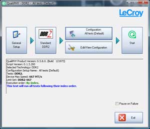
QualiPHY has many preset compliance configurations but also enables users to create their own configuration and limit sets.
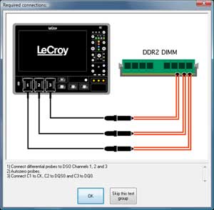
Connection Diagrams prompt the user to make the necessary connections..
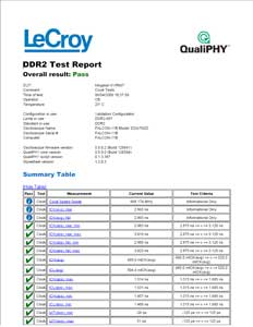
Compliance Reports contain all of the tested values, the specific test limits and screen captures. Compliance Reports can be created as HTML, PDF or XML.
QualiPHYQualiPHY is designed to reduce the time, effort and specialized knowledge needed to perform compliance testing on high-speed serial buses.
- Guides the user through each test setup
- Performs each measurement in accordance with the relevant test procedure
- Compares each measured value with the applicable specification limits
- Fully documents all results
- QualiPHY helps the user perform testing the right way -- every time!
Clock Tests
tCK(avg) – Average Clock Period
tCH(avg) – Average High Pulse Width
tCL(avg) – Average Low Pulse Width
tCK (abs) – Absolute Clock Period
tCH(abs) – Absolute High Pulse Width
tCL(abs) – Absolute Low Pulse Width
tJIT(duty) – Half Period Jitter
tJIT(per) – Clock Period Jitter
tJIT(cc) – Cycle to Cycle Period Jitter
tERR(n per) – Cumulative error
Electrical Tests
SlewR – Input Rising Edge Slew Rate
SlewF – Input Falling Edge Slew Rate
VIH(ac) – AC Input Logic High
VIH(dc) – DC Input Logic High
VIL(ac) – AC Input Logic Low
VIL(dc) – DC Input Logic Low
VSWING – Input Signal Maximum
Peak to Peak Swing
SoutR – Output Slew Rate Rise
SoutF – Output Slew Rate Fall
tSLMR – Output Slew Rate Matching Ratio
AC Overshoot Peak Amplitude
AC Overshoot Area Above VDDQ
AC Undershoot Peak Amplitude
AC Undershoot Area Below VSSQ
VID(ac) – AC Differential Input Voltage
VIX(ac) – AC Differential Input Cross Point Voltage
VOX(ac) – AC Differential Output Cross Point Voltage
Timing Tests
tHZ(DQ) – DQ High Impedance Time from CK/CK#
tLZ(DQ) – DQ Low Impedance Time from CK/CK#
tLZ(DQS) – DQS Low Impedance Time from CK/CK#
tHP – CK Half Pulse Width
tQHS – DQ Hold Skew Factor
tQH – DQ/DQS Output Hold Time from DQS
tDQSH – DQS Input High Pulse Width
tDQSL – DQS Input Low Pulse Width
tDSS – DQS Falling Edge to CK Setup Time
tDSH – DQS Falling Edge Hold Time from CK
tWPRE – Write Preamble
tWPST – Write Postamble
tRPRE – Read Preamble
tRPST – Read Postamble
tDQSQ – Skew between DQS and DQ
tDQSS – DQS Latching Transition to Clock Edge
tDQSCK – DQS Output Access Time from CK/CK#
tAC – DQ Output Access Time from CK/CK#
tDS(base) – DQ and DM Input Setup Time
tDH(base) – DQ and DM Input Hold Time
tIS(base) – Address and Control Input Setup Time
tIH(base) – Address and Control Input Hold Time
tDS1(base) – DQ and DM Input Setup Time (Single-ended Strobe)
tDH1(base) – DQ and DM Input Hold Time (Single-ended Strobe)
 STM32
STM32 MCU
MCU 通讯及无线技术
 物联网技术
物联网技术 电子DIY
电子DIY 板卡试用
板卡试用 基础知识
基础知识 软件与操作系统
 我爱生活
我爱生活 小e食堂
小e食堂