

ADC评估板核心是AD7606C-18,AD7606C-18是一款18位、同步采样、模数转换数据采集系统(DAS),具有八个通道。每个通道均包含模拟输入箝位保护、可编程增益放大器(PGA)、低通滤波器(LPF)和18位逐次逼近寄存器(SAR)模数转换器(ADC)。AD7606C-18还包含灵活的数字滤波器、低漂移、2.5 V精密基准电压源和用于驱动ADC的基准电压源缓冲区,以及灵活的并行和串行接口。
AD7606C-18采用5 V单电源供电,在所有通道以1 MSPS的吞吐量采样时,可适应以下输入范围:
双极单端:±12.5 V、±10 V、±6.25 V、±5 V和±2.5 V
单极单端:0 V至12.5 V、0 V至10 V和0 V至5 V
双极差分:±20 V、±12.5 V、±10 V和±5 V
输入箝位保护可承受高达±21 V的电压。由于采用单电源供电、片内滤波和高输入阻抗,因此无需外部驱动运算放大器(这些放大器需要双极电源)。对于吞吐率较低的应用,AD7606C-18灵活数字滤波器可用于提高噪声性能。
在硬件模式下,AD7606C-18与AD7608和AD7609完全兼容。在软件模式下,可以使用以下高级功能:
每个通道可选择模拟输入范围,并提供附加范围
每个通道可选择高带宽模式(220 kHz)
附加的过采样选项,过采样率高达256。
每通道的系统增益、系统失调和系统相位校准。
模拟输入开路检波器
诊断多路复用器
监测功能(串行外设接口(SPI)无效读和写、循环冗余校验(CRC)、持续忙碌监视器和复位检测)

框图如上,可以看到输入通道具有保护电路、PGA、LPF。

官网提供的原理图是空的,只有根据用户手册提供的说明使用了,官方手册使用的是EVAL-SDP-CH1Z (SDP-H1)这款FPGA开发板进行驱动,直接连接到底部HGDC接口。AD7606系列采用5V电源:

评估板带有转5V和3.3V LDO,通信逻辑接口电平是3.3V。

想要玩转开发板,首先就到弄明白板子的电源输入情况:

由于笔者手头没有SDP-H1控制板,因此需要将JP2接到B端,这样一来使用P4端子外部输入7~9V电源即可。

AD7606支持串行SPI和并行驱动,通过IO管脚选择,评估板默认是串行:

下面看看如果使用串行SPI接口,需要与主控连接的主要管脚:


总结如下:
RESET: 接MCU I/O, 配置输出模式,默认给低,高电平复位。
CONVST: 接MCU I/O,配置输出模式,当CONVST引脚从低电平转换为高电平时,ADC对模拟输入进行采样。
BUSY: 接MCU I/O, 配置输入模式,ADC转换完成时拉低。
FRSTDATA: 接MCU I/O, 配置输入模式,指示第一个通道V1正在回读(第18个时钟边沿后拉低)。这个管脚可以不接。
SPI配置为:模式2或者模式0
R_D_/SCLK: 串行时钟SCLK
DB9/DoutA:主机输入从机输出MISO
DB13/SDI: 主机输出从机输入MOSI
C_S_: 片选CS
再来看看数据手册描述的输入范围:

软件控制:

使用arduino驱动只需使用硬件SPI口即可。
#ifndef AD7606C_H
#define AD7606C_H

#include "arduino.h"
#include <SPI.h>

#define ADC_ALL_CH 8

#define PN20V0 0.00015258f
#define PN12V5 0.00009536f
#define PN10V0 0.00007629f
#define PN6V25 0.00004768f
#define PN5V00 0.00003815f
#define PN2V50 0.00001907f

#define PP12V5 0.00004768f
#define PP10V0 0.00003815f
#define PP5V00 0.00001907f
/*code to voltage*/
#define C2V(code, range_lsb) (code) * range_lsb

enum
{
  ADC_CH1 = 0x0,
  ADC_CH2 = 0x1,
  ADC_CH3 = 0x2,
  ADC_CH4 = 0x3,
  ADC_CH5 = 0x4,
  ADC_CH6 = 0x5,
  ADC_CH7 = 0x6,
  ADC_CH8 = 0x7
};

enum
{
  BIPOLAR_MODE = 0,
  UNIPOLAR_MODE = 1
};

class AD7606C
{
protected:
  uint8_t _RESET;
  uint8_t _CS;
  uint8_t _CONVST;
  uint8_t _FRSTDATA;
  uint8_t _BUSY;
  uint8_t _OS0;
  uint8_t _OS1;
  uint8_t _OS2;
  uint8_t _RANGE;
  uint8_t data_inc_status;
  void reset();
  void ipulse(uint8_t pin);

public:
  void setOversampling(uint8_t);
  void setRange(bool);
  // uint16_t debug_val;
};

class AD7606C_Serial : public AD7606C
{
protected:

#define HSPI_MISO D9
#define HSPI_MOSI D10
#define HSPI_SCLK D8
#define HSPI_SS D7


  SPIClass *hspi = NULL;
  uint8_t channel_mode[ADC_ALL_CH];

public:
  AD7606C_Serial(int CONVST, int BUSY);
  uint8_t read_reg(uint8_t, uint8_t *);
  uint8_t write_reg(uint8_t reg_addr, uint8_t reg_val);
  uint8_t write_and_chk_reg(uint8_t reg_addr, uint8_t reg_val);

  void convert_18bit_to_32bit(int32_t *unsigned_val, int32_t srcsz, int32_t *pdst);

  uint8_t data_read(int32_t *data);
  int32_t read(int32_t *data);    // Read raw values from ADC
  int32_t fast_read(int32_t *data); // fast read last conv raw values from ADC

  void config(void);
  void debug(void);
  uint8_t check_id(void);
  void get_all_reg_val(void);

  void test_reg_rw(void);
};

#endif
源码
#include "AD7606C.h"

#define AD7606_REG_STATUS 0x01
#define AD7606_REG_CONFIG 0x02
#define AD7606_REG_RANGE_CH_ADDR(ch) (0x03 + ((ch) >> 1))
#define AD7606_REG_BANDWIDTH 0x07
#define AD7606_REG_OVERSAMPLING 0x08
#define AD7606_REG_GAIN_CH(ch) (0x09 + (ch))
#define AD7606_REG_OFFSET_CH(ch) (0x11 + (ch))
#define AD7606_REG_PHASE_CH(ch) (0x19 + (ch))
#define AD7606_REG_DIGITAL_DIAG_ENABLE 0x21
#define AD7606_REG_DIGITAL_DIAG_ERR 0x22
#define AD7606_REG_OPEN_DETECT_ENABLE 0x23
#define AD7606_REG_OPEN_DETECTED 0x24
#define AD7606_REG_AIN_OV_UV_DIAG_ENABLE 0x25
#define AD7606_REG_AIN_OV_DIAG_ERROR 0x26
#define AD7606_REG_AIN_UV_DIAG_ERROR 0x27
#define AD7606_REG_DIAGNOSTIC_MUX_CH(ch) (0x28 + ((ch) >> 1))
#define AD7606_REG_OPEN_DETECT_QUEUE 0x2C
#define AD7606_REG_CLK_FS_COUNTER 0x2D
#define AD7606_REG_CLK_OS_COUNTER 0x2E
#define AD7606_REG_ID 0x2F

#define DATA_SIZE 28
// Reset the AD7606
void AD7606C::reset()
{
  digitalWrite(_RESET, 1);
  delayMicroseconds(1);
  digitalWrite(_RESET, 0);
  delayMicroseconds(1);
}

void AD7606C::setOversampling(uint8_t times)
{
  times > 6 ? times = 6 : times;
  pinMode(_OS0, OUTPUT);
  pinMode(_OS1, OUTPUT);
  pinMode(_OS2, OUTPUT);
  digitalWrite(_OS0, bitRead(B001, times));
  digitalWrite(_OS1, bitRead(B010, times));
  digitalWrite(_OS2, bitRead(B100, times));
}

void AD7606C::setRange(bool range)
{
  pinMode(_RANGE, OUTPUT);
  digitalWrite(_RANGE, range);
}
// Send a pulse to 0 or more pin for 1us
void AD7606C::ipulse(uint8_t pin)
{
  digitalWrite(pin, LOW);
  digitalWrite(pin, LOW); /* wait LP_CNV time */
  digitalWrite(pin, HIGH);
  digitalWrite(pin, HIGH);
}

AD7606C_Serial::AD7606C_Serial(int CONVST, int BUSY)
{
  _CONVST = CONVST;
  pinMode(_CONVST, OUTPUT);
  digitalWrite(_CONVST, 0);
  _BUSY = BUSY;
  pinMode(_BUSY, INPUT_PULLUP);

  hspi = new SPIClass(SPI);

  hspi->begin(HSPI_SCLK, HSPI_MISO, HSPI_MOSI, HSPI_SS);

  pinMode(hspi->pinSS(), OUTPUT);
  digitalWrite(hspi->pinSS(), HIGH);

  data_inc_status = 0;
}
// AD7606C_Serial::AD7606C_Serial(int FRSTDATA, int BUSY, int RESET)
// {
//  _RESET = RESET;
//  pinMode(_RESET, OUTPUT);
//  _BUSY = BUSY;
//  pinMode(_BUSY, OUTPUT);
//  _FRSTDATA = FRSTDATA;
//  pinMode(_FRSTDATA, INPUT);

//  hspi = new SPIClass(HSPI); // default 12:SPI2_MISO 13:SPI2_MOSI 14:SPI2_SCLK 15:SPI2_CS

// #ifndef ALTERNATE_PINS
//  // initialise hspi with default pins
//  // SCLK = 14, MISO = 12, MOSI = 13, SS = 15
//  hspi->begin();
// #else
//  // alternatively route through GPIO pins
//  hspi->begin(HSPI_SCLK, HSPI_MISO, HSPI_MOSI, HSPI_SS); // SCLK, MISO, MOSI, SS
// #endif
//  pinMode(hspi->pinSS(), OUTPUT); // VSPI SS
//  digitalWrite(hspi->pinSS(), HIGH);

//  data_inc_status = 0;
// }
// AD7606C_Serial::AD7606C_Serial(int FRSTDATA, int BUSY, int RESET, int OS0, int OS1, int OS2, int RANGE)
// {
//  _RESET = RESET;
//  pinMode(_RESET, OUTPUT);
//  _BUSY = BUSY;
//  pinMode(_BUSY, OUTPUT);
//  _OS0 = OS0;
//  pinMode(_OS0, OUTPUT);
//  _OS1 = OS1;
//  pinMode(_OS1, OUTPUT);
//  _OS2 = OS2;
//  pinMode(_OS2, OUTPUT);
//  _RANGE = RANGE;
//  pinMode(_RANGE, OUTPUT);
//  _FRSTDATA = FRSTDATA;
//  pinMode(_FRSTDATA, INPUT);

//  hspi = new SPIClass(HSPI); // default 12:SPI2_MISO 13:SPI2_MOSI 14:SPI2_SCLK 15:SPI2_CS

// #ifndef ALTERNATE_PINS
//  // initialise hspi with default pins
//  // SCLK = 14, MISO = 12, MOSI = 13, SS = 15
//  hspi->begin();
// #else
//  // alternatively route through GPIO pins
//  hspi->begin(HSPI_SCLK, HSPI_MISO, HSPI_MOSI, HSPI_SS); // SCLK, MISO, MOSI, SS
// #endif
//  pinMode(hspi->pinSS(), OUTPUT); // VSPI SS
//  digitalWrite(hspi->pinSS(), HIGH);

//  data_inc_status = 0;
// }

#define NO_OS_BIT(x) (1 << (x))
#define AD7606_RD_FLAG_MSK(x) (NO_OS_BIT(6) | ((x) & 0x3F))
#define AD7606_WR_FLAG_MSK(x) ((x) & 0x3F)

/**
 * @brief Read a device register via SPI.
 *
 * This function performs CRC8 computation and checking if enabled in the device.
 *
 * @param reg_addr   - Register address in device memory.
 * @param reg_val    - Pointer to the location where to store the register value.
 *
 * @return ret - return code.
 * @note   ad7606c-18 ds P.47
 */
uint8_t AD7606C_Serial::read_reg(uint8_t reg_addr, uint8_t *reg_val)
{
  static uint16_t data_temp;
  static uint8_t ret;
  // data_temp = (0x2 | (reg_addr & 0x3F) << 2) << 8;// 0x3F is mask 0bxx111111 shit!!!
  data_temp = AD7606_RD_FLAG_MSK(reg_addr) << 8;
  hspi->beginTransaction(SPISettings(1000000, MSBFIRST, SPI_MODE2));
  digitalWrite(hspi->pinSS(), LOW);  // pull SS slow to prep other end for transfer
  hspi->transfer16(data_temp);     // 发送第1帧
  digitalWrite(hspi->pinSS(), HIGH); // pull ss high to signify end of data transfer
  delayMicroseconds(1);
  digitalWrite(hspi->pinSS(), LOW);        // pull SS slow to prep other end for transfer
  *reg_val = hspi->transfer16(data_temp) & 0xFF; // 发送第2帧(与第1帧内容相同) 并且取低8位为寄存器内容
  digitalWrite(hspi->pinSS(), HIGH);         // pull ss high to signify end of data transfer
  hspi->endTransaction();
  return ret;
}

/**
 * @brief Write a device register via SPI.
 *
 * This function performs CRC8 computation and checking if enabled in the device.
 *
 * @param reg_addr   - Register address in device memory.
 * @param reg_data   - Value to write to register.
 *
 * @return ret - return code.
 *         Example: -EIO - SPI communication error.
 *                  -ENOTSUP - Device not in software mode.
 *                  -EBADMSG - CRC computation mismatch.
 *                  0 - No errors encountered.
 */
uint8_t AD7606C_Serial::write_reg(uint8_t reg_addr, uint8_t reg_val)
{
  static uint16_t data_temp;
  static uint8_t ret;
  static uint8_t debug;
  /* Dummy read to place the chip in register mode. */
  read_reg(reg_addr, &debug);
  data_temp = AD7606_WR_FLAG_MSK(reg_addr) << 8 | (reg_val & 0xFF);
  hspi->beginTransaction(SPISettings(2000000, MSBFIRST, SPI_MODE2));
  digitalWrite(hspi->pinSS(), LOW);     // pull SS slow to prep other end for transfer
  debug = hspi->transfer16(data_temp) & 0xFF; // 发送第1帧
  digitalWrite(hspi->pinSS(), HIGH);      // pull ss high to signify end of data transfer
  hspi->endTransaction();
  return ret;
}

uint8_t AD7606C_Serial::write_and_chk_reg(uint8_t reg_addr, uint8_t reg_val)
{
  static uint16_t data_temp;
  static uint8_t ret;
  static uint8_t debug;
  static uint8_t data_rd;
  /* Dummy read to place the chip in register mode. */
  read_reg(reg_addr, &debug);
  data_temp = AD7606_WR_FLAG_MSK(reg_addr) << 8 | (reg_val & 0xFF);
  hspi->beginTransaction(SPISettings(2000000, MSBFIRST, SPI_MODE2));
  digitalWrite(hspi->pinSS(), LOW);     // pull SS slow to prep other end for transfer
  debug = hspi->transfer16(data_temp) & 0xFF; // 发送第1帧
  digitalWrite(hspi->pinSS(), HIGH);      // pull ss high to signify end of data transfer
  hspi->endTransaction();
  read_reg(reg_addr, &data_rd);
  if (data_rd != reg_val)
  {
    Serial.printf("[error]reg write fail!\r\n");
    ret = 1;
  }
  return ret;
}

uint8_t AD7606C_Serial::check_id(void)
{
  uint8_t ret = 0;
  uint8_t byte1;

  read_reg(0x2F, &byte1);
  if ((byte1 & 0xF0) == 0x30)
  {
    if ((byte1 & 0x0F) != 0x02)
    {
      Serial.printf("[error]SILICON_REVISION is not 0x02, is:0x%x\r\n", byte1);
      ret = 2;
    }
    else
    {
       Serial.printf("DEV_ID:D7606C-18 generic. SILICON_REVISION:0x%x\r\n", byte1 & 0x0F);
    }
  }
  else
  {
    ret = 1;
    Serial.printf("[error]DEV_ID is not D7606C-18 generic or AD7606C Init fail! data:0x%x\r\n", byte1);
  }
  return ret;
}

void AD7606C_Serial::get_all_reg_val(void)
{
  uint8_t byte1;

  for (uint8_t i = 0x01; i < 0x30; i++)
  {
    read_reg(i, &byte1);
    Serial.printf("[debug]reg:0x%2x,data:0x%2x\r\n", i, byte1);
  }
}

static const uint16_t tconv_max[] = {
  1,   /* AD7606_OSR_1 */
  3,   /* AD7606_OSR_2 */
  5,   /* AD7606_OSR_4 */
  10,  /* AD7606_OSR_8 */
  20,  /* AD7606_OSR_16 */
  41,  /* AD7606_OSR_32 */
  81,  /* AD7606_OSR_64 */
  162, /* AD7606_OSR_128 */
  324  /* AD7606_OSR_256 */
};
/**
 * @enum ad7606_osr
 * @brief Oversampling ratio
 */
enum ad7606_osr
{
  /** Oversample by 1 */
  AD7606_OSR_1,
  /** Oversample by 2 */
  AD7606_OSR_2,
  /** Oversample by 4 */
  AD7606_OSR_4,
  /** Oversample by 8 */
  AD7606_OSR_8,
  /** Oversample by 16 */
  AD7606_OSR_16,
  /** Oversample by 32 */
  AD7606_OSR_32,
  /** Oversample by 64 */
  AD7606_OSR_64,
  /** Oversample by 128, available for chips that have software mode only */
  AD7606_OSR_128,
  /** Oversample by 256, available for chips that have software mode only */
  AD7606_OSR_256
};

void AD7606C_Serial::config(void)
{
  uint8_t byte1;

  check_id();
  write_and_chk_reg(AD7606_REG_CONFIG, 0x00); // CONFIG 0x02(数据中增加状态位,用于区分通道x的数据)
  // write_and_chk_reg(AD7606_REG_CONFIG, 0x02);data_inc_status = 1;
  write_and_chk_reg(AD7606_REG_BANDWIDTH, 0x00); // 全部使用低带宽
  // write_and_chk_reg(AD7606_REG_OVERSAMPLING, 0xF8); // 使用最大过采样率 AD7606_OSR_256 & OS_PAD = 16 => busy=494.6us
  write_and_chk_reg(AD7606_REG_OVERSAMPLING, 0x08);   // 使用最大过采样率 AD7606_OSR_256 & OS_PAD = 0  => busy=255.6us
  write_and_chk_reg(AD7606_REG_RANGE_CH_ADDR(1), 0xBB); // channel1 & channel2 => ±20 V differential range
  write_and_chk_reg(AD7606_REG_RANGE_CH_ADDR(3), 0x5B); // channel3  => ±20 V differential range channel4 => 0 V to 5 V single-ended range.
  write_and_chk_reg(AD7606_REG_RANGE_CH_ADDR(5), 0x65); // channel5  => 0 V to 5 V single-ended range channel6 => 0 V to 10 V single-ended range.
  write_and_chk_reg(AD7606_REG_RANGE_CH_ADDR(7), 0x15); // channel7  => 0 V to 5 V single-ended range channel8 => ±5 V single-ended range.

  channel_mode[ADC_CH1] = BIPOLAR_MODE;
  channel_mode[ADC_CH2] = BIPOLAR_MODE;
  channel_mode[ADC_CH3] = BIPOLAR_MODE;
  channel_mode[ADC_CH4] = UNIPOLAR_MODE;
  channel_mode[ADC_CH5] = UNIPOLAR_MODE;
  channel_mode[ADC_CH6] = UNIPOLAR_MODE;
  channel_mode[ADC_CH7] = UNIPOLAR_MODE;
  channel_mode[ADC_CH8] = BIPOLAR_MODE;

  write_reg(0, 0); // exti register mode & get into ADC mode
}

/* Internal function to copy the content of a buffer in 18-bit chunks to a 32-bit buffer by
 * extending the chunks to 32-bit size. */
static int32_t cpy18b32b(uint8_t *psrc, uint32_t srcsz, uint32_t *pdst)
{
  unsigned int i, j;

  if (srcsz % 9)
    return 1;

  for (i = 0; i < srcsz; i += 9)
  {
    j = 4 * (i / 9);
    pdst[j + 0] = ((uint32_t)(psrc[i + 0] & 0xff) << 10) | ((uint32_t)psrc[i + 1] << 2) | ((uint32_t)psrc[i + 2] >> 6);
    pdst[j + 1] = ((uint32_t)(psrc[i + 2] & 0x3f) << 12) | ((uint32_t)psrc[i + 3] << 4) | ((uint32_t)psrc[i + 4] >> 4);
    pdst[j + 2] = ((uint32_t)(psrc[i + 4] & 0x0f) << 14) | ((uint32_t)psrc[i + 5] << 6) | ((uint32_t)psrc[i + 6] >> 2);
    pdst[j + 3] = ((uint32_t)(psrc[i + 6] & 0x03) << 16) | ((uint32_t)psrc[i + 7] << 8) | ((uint32_t)psrc[i + 8] >> 0);
  }
  return 0;
}

/* Internal function to copy the content of a buffer in 26-bit chunks to a 32-bit buffer by
 * extending the chunks to 32-bit size. */
static int32_t cpy26b32b(uint8_t *psrc, uint32_t srcsz, uint32_t *pdst)
{
  unsigned int i, j;

  if (srcsz % 13)
    return 1;

  for (i = 0; i < srcsz; i += 13)
  {
    j = 4 * (i / 13);
    pdst[j + 0] = ((uint32_t)(psrc[i + 0] & 0xff) << 18) | ((uint32_t)psrc[i + 1] << 10) | ((uint32_t)psrc[i + 2] << 2) | ((uint32_t)psrc[i + 3] >> 6);
    pdst[j + 1] = ((uint32_t)(psrc[i + 3] & 0x3f) << 20) | ((uint32_t)psrc[i + 4] << 12) | ((uint32_t)psrc[i + 5] << 4) | ((uint32_t)psrc[i + 6] >> 4);
    pdst[j + 2] = ((uint32_t)(psrc[i + 6] & 0x0f) << 22) | ((uint32_t)psrc[i + 7] << 14) | ((uint32_t)psrc[i + 8] << 6) | ((uint32_t)psrc[i + 9] >> 2);
    pdst[j + 3] = ((uint32_t)(psrc[i + 9] & 0x03) << 24) | ((uint32_t)psrc[i + 10] << 16) | ((uint32_t)psrc[i + 11] << 8) | ((uint32_t)psrc[i + 12] >> 0);
  }
  return 0;
}

void AD7606C_Serial::convert_18bit_to_32bit(int32_t *unsigned_val, int32_t srcsz, int32_t *pdst)
{
  unsigned int i;
  for (i = 0; i < srcsz; i++)
  {               // #Twos Complement Output Coding
                  // Bipolar Analog Input Ranges
    if (channel_mode[i] == 0) // BIPOLAR_MODE
    {
      pdst[i] = (unsigned_val[i] & 0x00020000) ? (unsigned_val[i] | 0xFFFC0000) : unsigned_val[i];
    }
    else // UNIPOLAR_MODE
    {
      pdst[i] = unsigned_val[i];
    }
  }
}

/**
 * @brief Read conversion data.
 *
 * --TODO:-This function performs CRC16 computation and checking if enabled in the device.
 * If the status is enabled in device settings, each sample of data will contain
 * status information in the lowest 8 bits.
 *
 * The output buffer provided by the user should be as wide as to be able to
 * contain 1 sample from each channel since this function reads conversion data
 * across all channels.
 *
 * @param data       - Pointer to location of buffer where to store the data.
 *
 * @return ret     - return code.
 *         Example: 1 - xxx error.
 *                  0 - No errors encountered.
 */
uint8_t AD7606C_Serial::data_read(int32_t *data)
{
  uint8_t ret;
  uint32_t sz;
  int32_t i;
  uint16_t crc, icrc;
  uint8_t bits = 18;
  uint8_t sbits = data_inc_status ? 8 : 0;
  uint8_t nchannels = 8;
  uint32_t data_temp[DATA_SIZE];
  uint8_t data_buf[DATA_SIZE] = {0x00};

  sz = nchannels * (bits + sbits);

  /* Number of bits to read, corresponds to SCLK cycles in transfer.
   * This should always be a multiple of 8 to work with most SPI's.
   * With this chip family this holds true because we either:
   *  - multiply 8 channels * bits per sample
   *  - multiply 4 channels * bits per sample (always multiple of 2)
   * Therefore, due to design reasons, we don't check for the
   * remainder of this division because it is zero by design.
   */
  sz /= 8; // 不包含status时为18个

  memset(data_buf, 0, sz);

  digitalWrite(hspi->pinSS(), LOW); // pull SS slow to prep other end for transfer

  portDISABLE_INTERRUPTS();
  for (uint8_t i = 0; i < sz; i++)
  {
    data_buf[i] = hspi->transfer(0x00);
  }
  portENABLE_INTERRUPTS();
  digitalWrite(hspi->pinSS(), HIGH); // pull ss high to signify end of data transfer

  switch (bits)
  {
  case 18:
    if (data_inc_status)
    {
      ret = cpy26b32b(data_buf, sz, data_temp);
      // TODO:
    }
    else
    {
      ret = cpy18b32b(data_buf, sz, data_temp);
      convert_18bit_to_32bit((int32_t *)data_temp, 8, data);
    }

    if (ret)
      return ret;
    break;
  // case 16:
  //  for (i = 0; i < nchannels; i++)
  //  {
  //    if (data_inc_status)
  //    {
  //      data[i] = (uint32_t)dev->data[i * 3] << 16;
  //      data[i] |= (uint32_t)dev->data[i * 3 + 1] << 8;
  //      data[i] |= (uint32_t)dev->data[i * 3 + 2];
  //    }
  //    else
  //    {
  //      data[i] = (uint32_t)dev->data[i * 2] << 8;
  //      data[i] |= (uint32_t)dev->data[i * 2 + 1];
  //    }
  //  }
  //  break;
  default:
    ret = 1;
    break;
  };

  return ret;
}

/**
 * @brief Blocking conversion start and data read.
 *
 * This function performs a conversion start and then proceeds to reading
 * the conversion data.
 *
 * @param data       - Pointer to location of buffer where to store the data.
 *
 * @return ret - return code.
 *                  0 - No errors encountered.
 */
int32_t AD7606C_Serial::read(int32_t *data)
{
  int32_t ret;
  uint8_t busy;
  uint32_t timeout = tconv_max[AD7606_OSR_256];

  ipulse(_CONVST);
  /* Wait for BUSY falling edge */
  while (timeout)
  {
    if (digitalRead(_BUSY) == 0)
      break;

    delayMicroseconds(1);
    timeout--;
  }

  if (timeout == 0)
  {
    Serial.printf("[error]timeout\r\n");
    return 1;
  }

  return data_read(data);
}

int32_t AD7606C_Serial::fast_read(int32_t *data)
{
  int32_t ret;
  uint8_t busy;
  uint32_t timeout = tconv_max[AD7606_OSR_256];

  ipulse(_CONVST);

  data_read(data); // get last sample data
  /* Wait for BUSY falling edge */
  while (timeout)
  {
    if (digitalRead(_BUSY) == 0)
      break;

    delayMicroseconds(1);
    timeout--;
  }

  if (timeout == 0)
  {
    Serial.printf("[error]timeout\r\n");
    return 1;
  }

  return 0;
}寄存器定义:使用宏定义了芯片内部寄存器的地址,包括状态、配置、通道量程、带宽、过采样、增益、偏移、诊断等寄存器。
硬件控制:
reset():通过复位引脚产生脉冲复位芯片。
setOversampling():通过三个引脚设置过采样率(0~6倍)。
setRange():通过RANGE引脚设置输入量程(单极性/双极性)。
ipulse():向指定引脚发送短脉冲(用于触发转换)。
SPI通信:
read_reg() / write_reg():读写单字节寄存器,支持CRC校验(代码中未完整实现)。
write_and_chk_reg():写入后回读验证。
check_id():读取ID寄存器(0x2F)验证芯片型号。
get_all_reg_val():遍历读取所有寄存器并打印。
芯片配置:
config():执行典型初始化流程:检查ID、配置寄存器(如设置带宽、过采样、各通道量程),最后退出寄存器模式进入ADC模式。
数据读取:
data_read():从SPI读取原始数据(18位或26位,取决于是否包含状态位),解析并转换为32位有符号整数。
convert_18bit_to_32bit():将18位补码数据扩展为32位有符号数,处理双极性/单极性模式。
read():触发转换并等待BUSY信号,然后读取数据。
fast_read():先触发转换,然后读取上一次转换的结果(流水线操作)。
测试代码
#include "AD7606C.h"
#define ADC_CONVST D0
#define ADC_BUSY D1
int32_t adc_raw_data[ADC_ALL_CH];
float adc_disp_val[ADC_ALL_CH];
AD7606C_Serial AD7606C_18(ADC_CONVST, ADC_BUSY);
#define RESET D2 //out
#define FRSTDATA D3 //in First Data Output. The FRSTDATA output signal indicates when the first channel, V1, is being read back on the parallel interface or the serial interface.
void setup()
{
Serial.begin(9600);
pinMode(RESET, OUTPUT);
pinMode(FRSTDATA, INPUT);
digitalWrite(RESET, HIGH);
delay(1);
digitalWrite(RESET, LOW);
Serial.println("ad7606 config begin");
delay(100);
Serial.println("ad7606 config begin");
AD7606C_18.config();
Serial.println("ad7606 config end");
}
void loop()
{
AD7606C_18.fast_read(adc_raw_data);
adc_disp_val[ADC_CH1] = C2V(adc_raw_data[ADC_CH1], PP5V00);
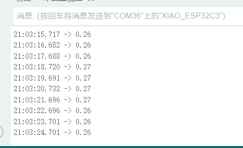
Serial.println(adc_disp_val[ADC_CH1]);
delay(1000);
}
 我要赚赏金
我要赚赏金 STM32
STM32 MCU
MCU 通讯及无线技术
 物联网技术
物联网技术 电子DIY
电子DIY 板卡试用
板卡试用 基础知识
基础知识 软件与操作系统
 我爱生活
我爱生活 小e食堂
小e食堂

