
OCIS codes: (260.0260) Physical optics; (260.2110) Electromagnetic optics; (260.1440) Birefringence; (230.4170) Multilayers.
https://doi.org/10.1364/AO.56.004566 1.引言
由平行平面构成的光学层在光学中广泛应用。层状结构可以用作许多不同情况的模型,像平板和标准具。基于这个事实,光与层状结构相互作用的主题一直引起大家的注意并且对此已经进行了大量的研究。
在这类研究中,大多数观点都侧重于平面波,然而仅仅少数的研究使用了平面波谱方法(SPW)来考虑一般的电磁场。例如,参考文献[1-6]中研究了各向同性-各向同性的界面上,高斯光束的反射率和透射率;在参考文献[7-11]中研究了各向同性层或者平板的情况;参考文献[12-22]讨论了各向同性-各向异性界面的情况,在参考文献[23-26]中则讨论了各向异性层或者平板的情况。
上面所提到的许多研究都用于特定的研究主题,像[1,3,5]中研究了高斯光束全内反射的横向偏移,并且他们常常关注于具体的配置。因此,将这些方法推广到更一般的情况的可能性受到了限制。
在这篇文章中,我们从一个更一般的观点来考虑此问题。光学层几乎不会单独使用;相反,他们常常是一个光学系统的一部分并且和其他的元件一起使用,如图1中所示。基于此事实,我们遵循场追迹的概念[27],并使用不同的场追迹算子组合[28-32],如图1中所示,以对一个包含了层介质元件的系统进行物理光学模拟。考虑到模拟是对整个系统而不是单个元件,仿真层结构必须与系统的前后部分相连接。这要求我们传播步骤(图1中的P)进行适当的考虑,将前一个元件的输出连接到当前元件的输入,并将当前元件的输出传递到下一个元件。一般情况下,这样的传输步骤会出现在平行或者非平行平面之间。在参考文献[28,29]中已经提到了平行平面间几种有效的传输方法,在参考文献[33]中则可以找到对非平行平面间传输的一个详细的讨论。在这篇文章中,我们不会研究传输步骤,但会关注层状结构的元件算子C。
此外,从数值计算的观点出发,为了执行一个连续且有效的系统模拟,要求元件算子C
正确地处理采样场数据并和其他的算子以一种统一的格式传递场数据;
优化数值计算的效率。
考虑到上述两个标准,我们开发了一种具有自动数值采样规则的SPW方法。与之前一些利用积分方法对空间和角谱相关的傅里叶变换进评估的研究相比(如参考文献[23]中的二维中点规则和参考文献[12-14,20,25]中的Stamnes–Spjelkavik–Pedersen方法[34]),我们使用了快速傅里叶变换(FFT)技术,此技术在大部分数值软件包中容易访问并且效率高。再加上在角谱域中经过深入考虑的数值采样规则,我们的方法具有一般适用性,对层元件和入射场没有任何限制。因此,此算法可以直接包含在一个物理光学系统模拟之中。
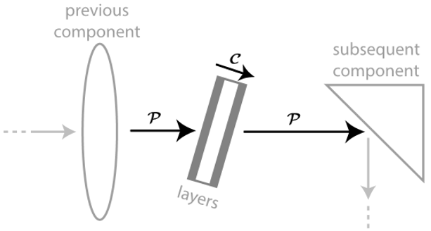 图1.结合使用不同的场追踪算子来模拟光学系统: C是元件算子,P是相邻元件之间的传输算子。 2.理论
如图2所示,层状结构分别由两个位于
 和
和 的平行平面构成。
 和
和 的区域充满了复折射率为
 和
和 的均匀各向同性介质。参考文献[27]中表明使用横向分量Ex和Ey已足够表征均匀各向同性介质中电磁场了。因此,我们可以使用以下表达式来描述此问题:
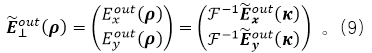
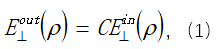 其中,分别在平面和处定义输入和输出横向电场矢量,(两者位于界面的数学位置,但总是认为在均匀介质的一侧),由下式给出
 其中
其中 。方程(1)中的元件算子是一个2x2的矩阵形式,
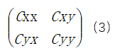
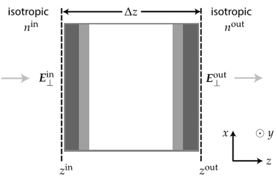 图2.层状结构分别由两个位于和的平行平面构成。和的区域由均匀各向同性介质填充,其折射率分别是和。输出场和输出场在层表面进行定义,但总是在相应的各向同性介质的一侧。 在这章节,我们的目标是找到C的精确的形式,以连接层介质元件的输入和输出场。为了研究与层结构的相互作用,我们对输入横向场分量进行了一个傅里叶变换,并获得了
 其中
其中 , F表示二维傅里叶变换,
 。逆傅里叶变换定义如下
 方程(6)中的积分可以解释为将
 分解为具有不同横向波矢分量κ的平面波。因此,在我们的情况下,每个输入平面波都可以单独处理——我们首先计算每个输入平面波的输出,然后进行求和从而获得输出场。此外,根据边界条件对电磁场施加的连续性要求,可以显示出一个给定的输入平面波在与层结构相互作用的过程中其横向波矢分量κ必定保持不变。同样可以显示出,通过叠加原理的有效性,不同的κ之间没有耦合。因此,对于输出角谱,我们可以写下
 其中
其中 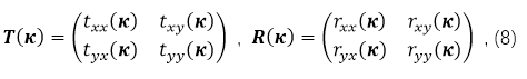
通过联合方程(4),(7),(9),我们可以写出从输入场到输出场整个计算流程,如果我们以透射的情况作为例子,则
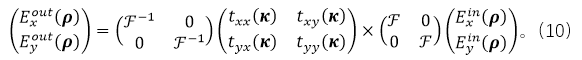 因此,方程(1)中元件算子C的精确形式如下
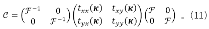
通过使用系数矩阵R(κ)代替 T(κ),可以获得反射情况的表达式。 3.算法
按照方程(10)的顺序,我们可以应用一种数值算法以计算场经过分层介质元件的传输。让我们从横向输入场矢量
 和
和 ,以图3(a)中的均匀网格进行采样。这种网格定义为
 ,其中
,其中 和
和 作为索引数,δx和δy是x方向和y方向的采样距离。初始采样参数应该受到合适的控制以使他们符合先前算子的奈奎斯特-香农采样定理。方程(10)中的F为联系空间域和频率域的算子,可以使用不同的数值方法实现,像广泛使用的快速傅里叶变换(FFT)技术,以及包含了能够进一步提高数值效率的半解析傅里叶变换[38]和啁啾z变换[39-41]的更高级的方法。在此篇文章中,我们使用了FFT技术,并以此获得输入角谱。但我们的算法不受限于该技术。
 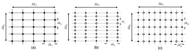 图3.在角谱域定义均匀采样网格。(a),初始网格定义,5x5采样点,
 和
和 为采样距离;(b),使用5x5采样点,沿垂直方向生成一个测试网格,和
 =0.5为采样距离;(c)中使用9x5个采样点定义了沿水平方向的一个测试网格,
 =0.5和为采样距离。((b)和(c)中的实心点是在(a)的初始网格中出现的共同的采样点位置,而空心圆环与初始网格中不一样的采样点。
 ,其中和为Kx和Ky的采样距离。利用FFT计算的结果,在两个域中的采样点是一样的,因此我们有
 。接下来,将输入角谱乘以系数矩阵,然后我们可以获得输出角谱场,例如,对于透射
 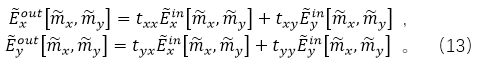 角谱
角谱 的采样通过傅里叶变换关系自动确保。然而,
 的采样没有必要进行确保,因为他们包含了系数和输入角谱之间的点乘。这个问题将在第四部分的案例中进行清楚地说明。一般来说,采样距离,和带宽
 必须进行适当调整以确保正确的采样。在我们的情况中,方程(13)中的运算没有改变谱范围。因此,我们仅仅只需要找到合适的采样距离即可。此问题并没有解析解,因为系数矩阵T或者R是通过递归S矩阵方法数值上获得的。确保采样的唯一方法是实行数值测试。
让我们在角谱域定义一个测试采样网格,如如3(b)或者3(c)所示。测试网格定义为
 ,其中
,其中 为指数;为了不改变角谱范围,要求
 。与初始网格相比,它也需要进行细化,这意味着
 。一方面,我们以一种严谨的方式来计算测试网格上的输出横向角谱分量。由于输入横向角谱分量的合适采样,根据需要可以进行插值,例如,在测试网格上,我们获得
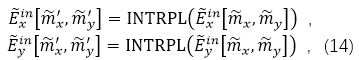 其中“INTRPL”代表的是数值插值运算。为了在一个更精细的网格上严格地获得输入场,如方程(14)中,我们总是采用基于FFT的Sinc插值方法,把它们代入到方程(13)中,可以严格地获得输出横向角谱量
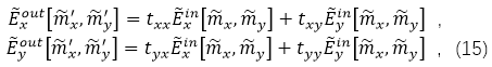 另一方面,通过对
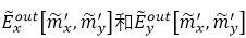 的插值,我们也可以获得测试网格上的输出横向角谱量,并将插值结果表示为
 。我们将此过程描述为
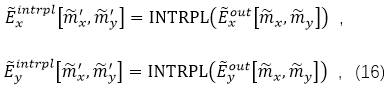 值得强调的是,在方程(16)中无需再使用严格的Sinc插值。因为这些结果仅仅用于评估一下情况。在这篇文章中,我们使用三次插值。上面的插值没必要给出正确的输出值,因此,在方程(16)的左边,我们对那些量使用上标“intrpl”。下一步,我们定义
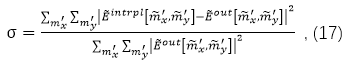 作为插值结果和严格结果之间的相对偏差。只要
 在初始网格上的采样满足奈奎斯特-香农采样定理,基于他们的插值结果就不会对严格的插值方法表现出一个大的偏差。在这种情况下,根据所选的插值方法,两种结果的偏差应该在数值误差级次,由σ_0表示。使用上述标准,通过一步步的减小采样间距来测试场采样,直至σ<σ_0。
以上的测试过程对应着一个循环,在每个测试循环中都会执行方程(14)到(17)的计算。为了在每个测试循环中充分地使用测试数据,如方程(15)中的结果,我们总是使用图3(b)和3(c)中的测试网格。这样规则的测试网格定义为
对每个循环内,需要对先前的采样距离减半。使用这个测试网格具有如下好处:当计算
 时,仅仅需要计算那些在空心圆圈位置处的值,而实心点位置处的值在之前的测试循环中已经计算过了,并且让这些值简单地进行传输即可。在这种方式下,这些基于测试目的所进行严格计算的值不会被丢掉,而会作为下一次循环中的起始点以重新使用。因此,在一个完整的计算中所执行的是严格的计算,从而验证合适的采样,并且这些计算的值能够有效地用于构建最终输出场。我们将上面的方法总结在算法1中。算法1:通过合适的采样控制来进行输出角谱计算的数值流程1)在初始网格严格地计算2)初始化相对误差值σ=+∞3)判断σ>σ_0, ⊳如果为真,则采样不合适4)沿Kx(或者Ky)二等分采样距离5)应用新的采样距离定义测试网格
 6)在测试网格中对输入角谱插值,根据方程(14)获得
 7)根据方程(15),在测试网格上严格地计算输出角谱
 8)根据方程(16),通过插值获得
 9)根据方程(17),计算误差σ10)如果σ>σ_(0 )
  ,则⊳将目前的输出场设置为下一次循环的起始点11)返回 为了有效地处理非对称情况,例如,光束在x方向和y方向有不同的发散角,算法1中的测试需要按顺序沿两个方向进行。开始方向的选择是任意的,在我们的情况中,我们是沿y方向开始测试的。 4.示例
在VirtualLab Fusion[42]软件中,我们将第三节中提出的算法实现在“可编程元件”的编程界面中。这个元件可以与VirtualLab Fusion中其它的物理光学仿真技术进行联合仿真。接下来,我们展示了四个案例:前两个主要关注元件本身并以一种严格的数值方式检查此算法;后两个案例中,元件将用于光学系统中,例如,此算法与其它仿真技术一起使用。
在进入实际的案例之前,设置方程(17)中的迭代终止标准σ_0很重要。对于在此文中所使用的三次插值,我们预先检查了它在一般情况下的表现并在我们的数值环境中找到了一个0.01的基准值。 A.各向同性标准具
第一个案例模拟了一个线性偏振高斯光束经过一个标准具的传输。通过这个案例,我们将清楚的指出第三节中所说的采样问题并描述了算法1的工作原理。标准具由熔融石英制成,两侧有多层薄膜,如图4所示。关于标准具的光学参数和结构的更多信息,请见表1。输入场为波长633nm,x方向线偏光的高斯光束。其在元件的输入平面定义为E_⊥^in,且束腰半径为(2um,2um)。在经过傅里叶变换后,我们获得其角谱,同样具有高斯轮廓,如图5所示。按照方程(10)中的操作算子序列,输入角谱将乘以透射或者反射率系数。我们仍以透射作为例子,并且对于线性偏振输入场,我们使用t_xx和t_yx乘以E ̃_x^in,以获得输出角谱分量。
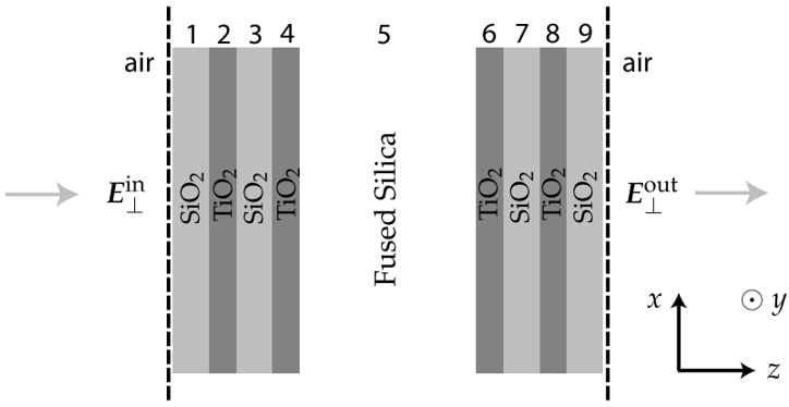 图4.由熔融石英制成,两侧有多层膜的标准具。其结构和光学参数如表1中所示。 表1 标准具的结构和光学参数
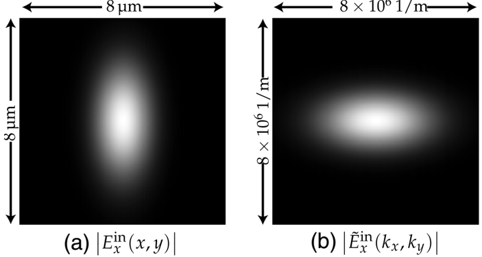 图5 .(a)输入高斯场分量的振幅;(b)对应的角谱分量。由于输入光场为沿x方向的线性偏振光,因此仅显示Ex分量。 如第三节中所指出,乘积
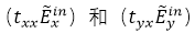 的采样不能自动得到保证,此案例中将显示该现象。标准具由于其频率选择功能(频谱或角频率)而得到广泛的使用。在我们的案例中,角频率选择可以解释为系数txx和tyx以一种方式调制输入角谱,以使特定的角频率加强而其它的减弱。这种调制可以出现在一种非常精细的频率水平上。因此,需要使用更精细的采样以在输出角谱中解析这样一个精细的调制。为了获得需要的采样间距,我们遵循算法1,图6中显示了部分结果。
通过图6和表2,我们根据算法1中的步骤描述了工作流程,如下:
第一步:从图6(a)中所示的输入角谱开始,计算各个系数并乘上元件矩阵以生成初始化的输出角谱;第二步:初始化相对偏差σ=+∞;第三步:开始测试循环;第四&五步:将采样距离沿κ_x或者κ_y方向减半,以定义测试网格
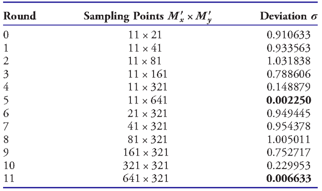
,对应的采样点如表2中所示;第六步:对输入角谱在测试网格上插值;第七步:在测试网格上严格的计算输出角谱,在此例中,对应图6(e);第八步:执行插值以获得,在此例中对应图6(b)-6(d);第九步:比较严格仿真和插值结果,并计算相对误差;第十步:对于较差的插值结果,如6(b)和6(c),表2中的0-3行,其结果是σ>σ_0,严格的结果将会传递给下一个循环并用于输入;否则,返回当前的结果。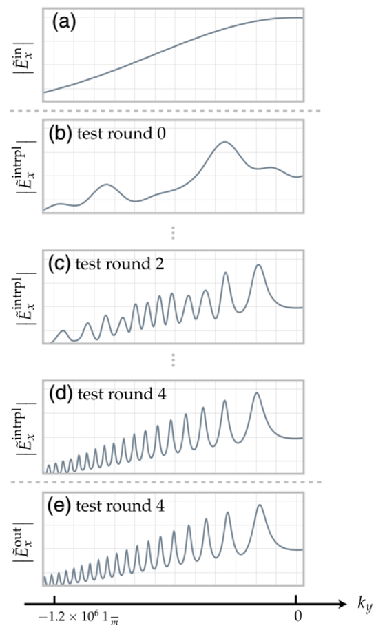 图6.算法1中不同步骤时沿κ_x方向的一维提取结果:(a)输入角谱振幅,(b)-(d),在测试循环中的插值角谱振幅以及(e)在最后的循环中严格地计算输出角谱。所有的子图中的值都缩放到相同的范围内。 从表2中我们也可以看到测试首先是沿y方向,之后再沿x方向执行的,如第三节的最后所提到的。从第0轮到第4轮测试,采样距离δκx并没有改变,因此采样点Mx^,保持不变;在第四轮测试后σ<σ0,沿y方向的测试终止,意味着场数据已经可以从先前一轮的结果中恢复。因此,沿y方向的采样点数是705,在第四轮中额外的704个数据仅仅是用于测试目的,对最终的输出并没有贡献。然后以一种类似的方式沿x方向开始测试并在第11轮终止,同样,场数据可以从先前一轮的结果中恢复。因此,最终输出的采样点数固定在2817x705。在表2的测试轮中,包含的总的采样点数是5633x705+45x704,数据45x704来自于沿y方向的最后测试轮。再次强调一下,为了在角谱域进行合适的采样,有必要采用如此大的采样点数。并且,除了沿x方向或者y方向最后一轮测试,用于测试目的而所有严格计算地值都用于构建最终输出场。 表2 Etalon模拟中每个测试轮次中的采样参数和误差
 文章中的模拟,使用的是一台Intel Core i7-4910MQ处理器,2.9GHz,32Gb物理内存的电脑。表2中所显示的示例所需的总的计算时间是118s。注意计算时间最多的部分是花在S矩阵计算上,而最后步骤的傅里叶逆变换仅花了约0.5s。
从表2中也可以看出沿x方向和沿y方向的测试轮次数也不一样,即沿两个方向所需的采样间距不同。因此,我们在算法中更倾向沿每个方向分别执行采样测试。
通过这个算法,我们获得了标准具的透过场,如图7所示。除了图7中透射场的尺寸远大于图5中的输入场,非零输出场分量
 也值得注意,尽管其振幅要远小于
 。Ex和Ey之间出现的偏振串扰是由于系数矩阵T或者R的非对角形式造成的。从的振幅分布中,还可以看出精细的同心圆,这是由于标准具多层结构中发生的多重反射造成的。
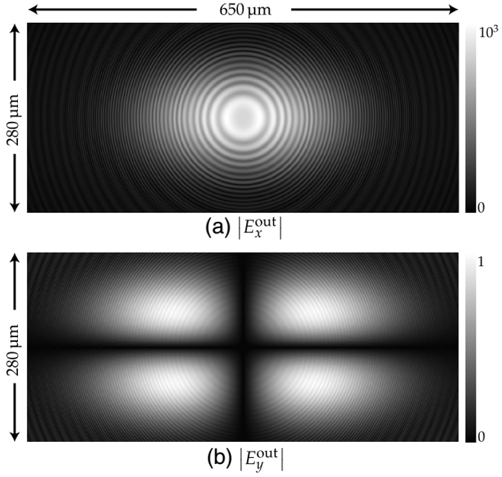 图7.以任意单位给出的标准具输出场分量的振幅,(a):|E_x^out |,(b):|E_y^out | B.单轴晶体板
我们的方法对各向同性介质层和各向异性介质层都同样适用。在这个案例中,我们演示了聚光干涉仪的原理,其可以用于精确的测量单轴晶体的光轴倾斜角度[43]。当使用会聚单色光照射正交偏振器间的晶体时,即可产生聚光干涉。图8中展示了聚光干涉仪的简要原理。在我们的模拟中,光源是一个Ex线性偏振,波长为633nm,NA=0.25的球面波,在晶体板前20mm。光源将输入场
 传递到晶体板的前表面,后表面的输出场将被分析。在这个子节中,我们没有讨论晶体板元件外部区域的传播步骤。
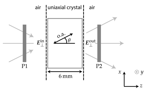 图8.使用聚光干涉仪测量光轴的角度。偏振片P1沿x方向,偏振片P2沿y方向,光轴表示为“o.a”。
我们使用聚光干涉仪,测试了一个6mm厚的向列液晶板,其光轴与z轴成θ角。其中n_e=1.7,n_0=1.5[43],设θ=0°,2°以及5°,我们观察了晶体板后y方向的输出场,如图9所示。当θ=0°,晶体的光轴垂直于晶体板表面,同心环的原点位于中心,如图9(a)所示;当θ≠0°时,如此例中的图9(b)和
图9(c),同心环的原点相应的发生了横向偏移。我们在模拟中获得的值与参考文献[43]中分析的结果一致。
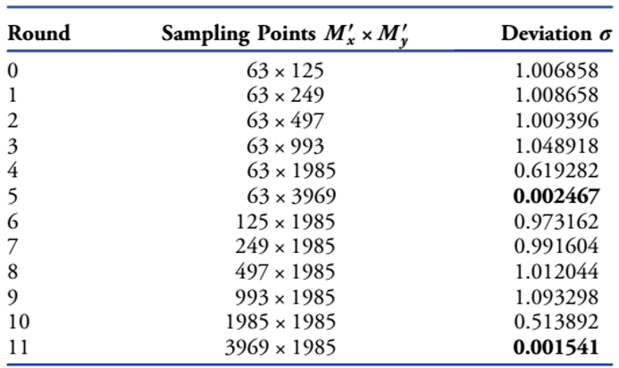
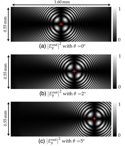 图9.针对不同的θ值,在晶体板后表面的输出场分布(振幅平方)。使用沿y方向的偏振片P2分析输出场,因此仅显示了E_y分量。红色的十字标出了同心圆环的原点,为(0,0),(210um,0)以及(525um,0),分别对应子图(a),(b)和(c)。 为了获得图9中的透射场,算法1再次被用于确定采样距离。为了完整性,表3中给出了θ=5°时此例中采样距离的数值测试的细节。在表3所显示的测试轮次中,包含了3969x1985+63x1984个采样点,对于每个采样点,计算了各向异性S矩阵,耗时416s。
表3.光轴为5°的单轴晶体板在每个测试轮次中的采样距离和偏差
C.倾斜的各向异性晶体板系统
如第一节所述,我们开发的算法是系统建模的一部分。在这个例子中,我们模拟了一个包含方解石晶体板的光学系统以研究偏振转换以及涡旋的生成[44],如图10所示。因为是针对整个系统进行建模,因此在处理过程使用了几种不同的场追迹算子[27]:偏振片使用琼斯矩阵算子,透镜被当作是理想透镜,到倾斜方解石板表面的光场传输使用参考文献[33]中的技术,方解石板中的光场传输则使用了此文中的方法。根据参考文献[44],给出了方解石晶体折射率,其中
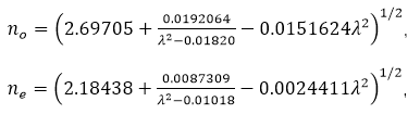
 图10.包含倾斜晶体板的系统。晶体板材料为方解石,厚度为6mm,光轴在图中以“o.a.”表示,垂直于晶体板表面。偏振片P1用于生成沿x方向的偏振光,而偏振片P2用于分析。透镜L1和L2焦距都为30mm。 此例中我们从α=0°开始,在系统中几个位置的场分布如图11所示。在偏振片P1前的输入场为波长633nm,x方向和y方向束腰半径1.5mm的高斯光束。经过偏振片P1之后,获得了一个沿x方向的线性偏振场。透镜L1后的聚焦场是方解石晶体板的输入场。根据算法1,我们获得了晶体板后表面的输出场,如图11(a)和11(b)。最后,在偏振片P2之后的平面上,我们获得了系统的输出场,如图11(c)和11(d)所示。
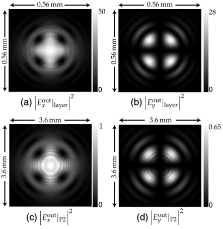 图11.图10中方解石晶体板及P2偏振片后的场分布(振幅平方),此例中α=0°。
让我们来仔细地观察一下图11中所展现的结果。数值测试细节在表4中给出。与4A部分的情况相似,由于T或者R的非对角线形式,沿x方向的线性偏振输入场为输出场增加了一个非零y偏振方向。但此例中单轴晶体板的偏振串扰相对更强,E(x )≈E(y ),而在标准具的例子中,E(x )和E(y )的比例大概是1000:1,如图7(a)和7(b)。这是由于方解石晶体的双折射性质,导致E(x )和E(y )分量之间具有一个强的耦合。
表4 1.5mm高斯光束入射到单轴晶体板,在每个测试轮次中的采样距离和偏差
P2后的场,如图11(e)和11(f)所示,与参考文献[44]中的测量结果吻合的很好。除了由双折射引起的四极结构,我们同样也看到了叠加在其上的同心圆环结构。与图11的分析类似,这些精细结构是由于板内的多重反射造成的。可以在参考文献[44]中的图4中看到同样的影响,尽管实验测量的对比度较低。
下一步,如参考文献[44]中所展示,我们将晶体倾斜一定的角度α并将输入高斯束腰设置为0.5mm,以生成单极光涡旋。模拟中,我们使用[33]中的方法处理非平行板之间的传输。通过这种方式,可以获得倾斜晶体板表面的输入场,且倾斜板表面的输出场可以继续传输至下一个元件。模拟结果如图12和13所示。当α=1.2°时,可以在表5中获得采样距离的数值测试细节。可以看到,沿x方向和y方向的偏差σ分别在轮次2和5中满足停止判据。我们沿两个方向继续往前迭代一次(标记有*)以获得一个过采样,以为了更好的与之后的非平行平面间的传播相结合[33],这之间的传播通常需要过采样因子为2.
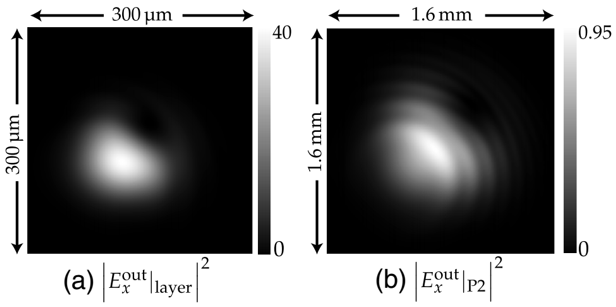 图12.当α=0.8°时,方解石晶体板和偏振片P2之后的输出场(振幅平方) 图12和13再次与参考文献[44]中的结果一致。与之前分析α=0°时的情况类似,光涡旋结构是由方解石晶体的双折射产生的。如图13(c)和13(d)所示,同样也可以看到相位错位引起的光涡旋。除了涡旋,图13(b)中还可以看到环形的精细结构,这是由于晶体板内的多重反射造成的。将表5中的数据测试与之前的进行比较,我们可以看到一个更快的收敛,特别是沿x方向的测试。包括表5中的所有测试循环,经过倾斜的方解石晶体板的传输仅使用了大约4s的计算时间就完成了,而整个系统的模拟,包含透镜,大约是30s的时间。由于方解石板绕y轴倾斜1.2°,若将晶体板表面作为参考,则对应着一个轻微的倾斜入射场。根据傅里叶变换偏移理论,沿y方向的倾斜将导致角谱沿此方向有一个偏移。因此,透射场的角谱同样存在沿x方向和y方向的不同调制。
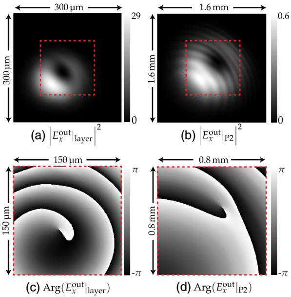 图13.当α=1.2°时,方解石晶体板和偏振片P2后的输出场,其中(a)和(b)为振幅平方的分布,(c)和(d)为相位分布 表5 0.5mm高斯光束入射到倾斜晶体板时,每轮测试中的采样参数和偏差
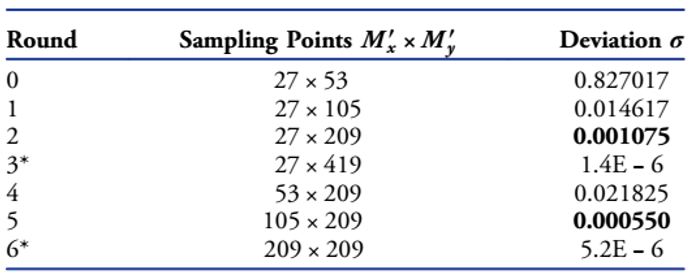
D.在空气-单轴表面的反射
对于反射情况,同样能以类似于算法中的透射情况的方法进行处理,我们将在下文展示。我们选用文献[45]的工作,即空气-单轴晶体表面发生的自旋霍尔效应,来作为一个例子。系统原理图如图14所示,且自旋相关纳米量级偏移可以通过检查反射场的中心来进行测量。
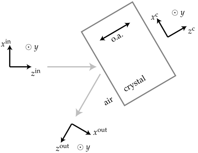 图14.在空气-单轴晶体表面的反射。晶体元件使用
 坐标系统来表示,其光轴(o.a.)沿
 方向,输入和反射场分在
 中给出 在我们的模拟中,使用了波长为632.8nm的线性偏振高斯场作为输入场,在此波长下,对于o光和e光,LiNbO3晶体样品的折射率分别为n0=2.232和ne=2.156。在文献[45]中并没有给出输出光场的光束尺寸,我们将其设置为20um。由于反射场的横向偏移是由空间频率域中的局部线性相位决定的,因此不改变光束尺寸的大小。
为了研究此效应,反射矢量场投影在圆偏单位矢量坐标系,而后我们测量了右旋圆偏振分量的中心。此外,对Ex和Ey两个线性偏振入射场,我们旋转晶体元件并监控位移随着入射角度的变化。模拟结果如图15中所示。我们使用参数扫描获得图15中的结果。对于每个入射角度,我们使用我们的算法计算了反射场,且在一个大的角度范围内显示出了较好的适应性。模拟结果与[45]中的结果匹配的很好。
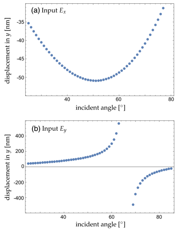 图15.入射角度与右圆偏振量反射场的横向偏移之间的关系,(a)Ex和(b)Ey分别为线性偏振输入。 总结
我们从系统仿真的角度研究了电磁场经过各向同性或各向异性层介质元件的传输。利用SPW分析并将以方程(10)的形式概括的结果,以为后续的数值实现做准备。我们清楚地讨论了在很多实际问题中会遇到的采样问题,此外,我们提出了一种数值测试算法,以更有效地在角谱域确定采样参数。通过标准具的案例,我们详细地描述了我们的算法的工作流程,显示了我们方法的一般有效性。此方法已经成功地应用到了对激光晶体封装技术中的应力诱导双折射的分析[46]。 致谢
我们感谢Olga Baladron-Zorita女士对此文章的校正以及其日常的帮助。 参考文献
B. R. Horowitz and T. Tamir, “Lateral displacement of a light beam at a dielectric interface*,” J. Opt. Soc. Am. 61, 586–594(1971).M. McGuirk and C. K. Carniglia, “An angular spectrum representation approach to the Goos–Hänchen shift,” J. Opt. Soc. Am. 67, 103–107(1977).S. Kozaki and H. Sakurai, “Characteristics of a Gaussian beam at a dielectric interface,” J. Opt. Soc. Am. 68, 508–514 (1978).C. C. Chan and T. Tamir, “Angular shift of a Gaussian beam reflected near the Brewster angle,” Opt. Lett. 10, 378–380 (1985).F. I. Baida, D. V. Labeke, and J.-M. Vigoureux, “Numerical study of the displacement of a three-dimensional Gaussian beam transmitted at total internal reflection near-field applications,” J. Opt. Soc. Am. A17, 858–866 (2000).S. Zhang, D. Asoubar, F. Wyrowski, and M. Kuhn, “Efficient and rigorous propagation of harmonic fields through plane interfaces,”Proc. SPIE 8429, 84290J (2012).M. Tanaka, K. Tanaka, and O. Fukumitsu, “Transmission and reflection of a Gaussian beam at oblique incidence on a dielectric slab,” J. Opt. Soc. Am. 67, 819–825 (1977).S. Kozaki and H. Harada, “Beam displacement of a reflected beam at an interface between an inhomogeneous medium and free space,”J. Opt. Soc. Am. 68, 1592–1596 (1978).C. W. Hsue and T. Tamir, “Lateral displacement and distortion of beams incident upon a transmitting-layer configuration,” J. Opt.Soc. Am. A 2, 978–988 (1985).R. P. Riesz and R. Simon, “Reflection of a Gaussian beam from a dielectric slab,” J. Opt. Soc. Am. A 2, 1809–1817 (1985).T. Tamir, “Nonspecular phenomena in beam fields reflected by multilayered media,” J. Opt. Soc. Am. A 3, 558–565 (1986).J. J. Stamnes and D. Jiang, “Focusing of electromagnetic waves into a uniaxial crystal,” Opt. Commun. 150, 251–262 (1998).J. J. Stamnes and V. Dhayalan, “Transmission of a two-dimensional Gaussian beam into a uniaxial crystal,” J. Opt. Soc. Am. A 18,1662–1669 (2001).J. J. Stamnes and V. Dhayalan, “Double refraction of a Gaussian beam into a uniaxial crystal,” J. Opt. Soc. Am. A 29, 486–497(2012).L. I. Perez, “Reflection and non-specular effects of 2d Gaussian beams in interfaces between isotropic and uniaxial anisotropic media,” J. Mod. Opt. 47, 1645–1658 (2000).L. I. Perez, “Nonspecular transverse effects of polarized and unpolarized symmetric beams in isotropic-uniaxial interfaces,” J. Opt. Soc.Am. A 20, 741–752 (2003).S. Stallinga, “Axial birefringence in high-numerical-aperture optical systems and the light distribution close to focus,” J. Opt. Soc. Am.A 18, 2846–2859 (2001).S. Stallinga, “Light distribution close to focus in biaxially birefringent media,” J. Opt. Soc. Am. A 21, 1785–1798 (2004).M. Jain, J. Lotsberg, J. Stamnes, and Ø. Frette, “Effects of aperture size on focusing of electromagnetic waves into a biaxial crystal,” Opt.Commun. 266, 438–447 (2006).M. Jain, J. K. Lotsberg, J. J. Stamnes, Ø. Frette, D. Velauthapillai, D.Jiang, and X. Zhao, “Numerical and experimental results for focusing of three-dimensional electromagnetic waves into uniaxial crystals,”J. Opt. Soc. Am. A 26, 691–698 (2009).S. Zhang and F. Wyrowski, “Simulations of general electromagnetic fields propagation through optically anisotropic media,” Proc. SPIE 9630, 96300A (2015).D. Asoubar, S. Zhang, and F. Wyrowski, “Simulation of birefringenceeffects on the dominant transversal laser resonator mode caused by anisotropic crystals,” Opt. Express 23, 13848–13865(2015).G. D. Landry and T. A. Maldonado, “Gaussian beam transmission and reflection from a general anisotropic multilayer structure,” Appl. Opt.35, 5870–5879 (1996).V. Dhayalan and J. J. Stamnes, “Focusing of electromagnetic waves into a dielectric slab, I: exact and asymptotic results,” Pure Appl. Opt.7, 33–52 (1998).V. Dhayalan and J. Stamnes, “Focusing of electromagnetic waves into a dielectric slab, II: numerical results,” J. Eur. Opt. Soc. 6,11036 (2011).A. Turpin, Y. V. Loiko, T. K. Kalkandjiev, and J. Mompart, “Light propagation in biaxial crystals,” J. Opt. 17, 065603 (2015).F. Wyrowski and M. Kuhn, “Introduction to field tracing,” J. Mod. Opt.58, 449–466 (2011).D. Asoubar, S. Zhang, F. Wyrowski, and M. Kuhn, “Parabasal field decomposition and its application to non-paraxial propagation,”Opt. Express 20, 23502–23517 (2012).D. Asoubar, S. Zhang, F. Wyrowski, and M. Kuhn, “Efficient semianalytical propagation techniques for electromagnetic fields,”J. Opt. Soc. Am. A 31, 591–602 (2014).H. Zhong, S. Zhang, and F. Wyrowski, “Parabasal thin-element approximation approach for the analysis of microstructured interfaces and freeform surfaces,” J. Opt. Soc. Am. A 32, 124–129 (2015).F. Wyrowski, H. Zhong, S. Zhang, and C. Hellmann, “Approximate solution of Maxwell’s equations by geometrical optics,” Proc. SPIE9630, 963009 (2015).F. Wyrowski and C. Hellmann, “Geometrical optics reloaded,”Optik Photonik 10, 43–47 (2015).S. Zhang, D. Asoubar, C. Hellmann, and F. Wyrowski, “Propagation of electromagnetic fields between non-parallel planes: a fully vectorial formulation and an efficient implementation,” Appl. Opt. 55, 529–538 (2016).34. J. J. Stamnes, B. Spjelkavik, and H. M. Pedersen, “Evaluation of diffraction integrals using local phase and amplitude approximations,”Opt. Acta 30, 207–222 (1983).D. W. Berreman, “Optics in stratified and anisotropic media:4 × 4-matrix formulation,” J. Opt. Soc. Am. 62, 502–510 (1972).L. Li, “Reformulation of the Fourier modal method for surface-relief gratings made with anisotropic materials,” J. Mod. Opt. 45,1313–1334 (1998).L. Li, “Note on the s-matrix propagation algorithm,” J. Opt. Soc. Am. A20, 655–660 (2003).Z. Wang, “Analytical handling of optical wavefront,” Master’s thesis(Friedrich Schiller University, 2015).L. Rabiner, R. Schafer, and C. Rader, “The chirp z-transform algorithm,” IEEE Trans. Audio Electroacoust. 17, 86–92 (1969).J. L. Bakx, “Efficient computation of optical disk readout by use of the chirp z transform,” Appl. Opt. 41, 4897–4903 (2002).M. Leutenegger, R. Rao, R. A. Leitgeb, and T. Lasser, “Fast focus field calculations,” Opt. Express 14, 11277–11291 (2006).Physical optics design software, “Wyrowski virtuallab fusion,” developed by Wyrowski Photonics UG, distributed by LightTrans GmbH. http://www.lighttrans.com.B. L. V. Horn and H. H. Winter, “Analysis of the conoscopic measurement for uniaxial liquid-crystal tilt angles,” Appl. Opt. 40, 2089–2094(2001).Y. Izdebskaya, E. Brasselet, V. Shvedov, A. Desyatnikov, W.Krolikowski, and Y. Kivshar, “Dynamics of linear polarizationconversion in uniaxial crystals,” Opt. Express 17, 18196–18208(2009).Y. Qin, Y. Li, X. Feng, Z. Liu, H. He, Y. Xiao, and Q. Gong, “Spin Hall effect of reflected light at the air-uniaxial crystal interface,” Opt.Express 18, 16832–16839 (2010).P. Ribes-Pleguezuelo, S. Zhang, E. Beckert, R. Eberhardt, F.Wyrowski, and A. Tünnermann, “Method to simulate and analyse induced stresses for laser crystal packaging technologies,” Opt.Express 25, 5927–5940 (2017).
 我要赚赏金
我要赚赏金 STM32
STM32 MCU
MCU 通讯及无线技术
 物联网技术
物联网技术 电子DIY
电子DIY 板卡试用
板卡试用 基础知识
基础知识 软件与操作系统
 我爱生活
我爱生活 小e食堂
小e食堂

