FSMCS RAM读写,跟LCD操作相似。
SRAM初始化之后,直接写数据在一个SRAM范围内的地址就行了,操作相对方便。
LCD相当于在一个固定的SRAM地址读写数据。
根据电路,SRAM使用了FSMC Bank1的SRAM3块。SRAM的基地址是0x68000000,因此定义:
#define Bank1_SRAM3_ADDR ((uint32_t)0x68000000)
下面是我的SRAM初始化程序和读写函数:
void My_SRAM_Init(void)
{
FSMC_NORSRAMInitTypeDef FSMC_NORSRAMInitStructure;
FSMC_NORSRAMTimingInitTypeDef p;
GPIO_InitTypeDef GPIO_InitStructure;
//时钟使能
RCC_APB2PeriphClockCmd(RCC_APB2Periph_GPIOD | RCC_APB2Periph_GPIOG | RCC_APB2Periph_GPIOE |
RCC_APB2Periph_GPIOF, ENABLE);
/*-- GPIO 设置 ------------------------------------------------------*/
/*!< 数据线配置 */
GPIO_InitStructure.GPIO_Pin = GPIO_Pin_0 | GPIO_Pin_1 | GPIO_Pin_8 | GPIO_Pin_9 |
GPIO_Pin_10 | GPIO_Pin_14 | GPIO_Pin_15;
GPIO_InitStructure.GPIO_Mode = GPIO_Mode_AF_PP;
GPIO_InitStructure.GPIO_Speed = GPIO_Speed_50MHz;
GPIO_Init(GPIOD, &GPIO_InitStructure);
GPIO_InitStructure.GPIO_Pin = GPIO_Pin_7 | GPIO_Pin_8 | GPIO_Pin_9 | GPIO_Pin_10 |
GPIO_Pin_11 | GPIO_Pin_12 | GPIO_Pin_13 | GPIO_Pin_14 |
GPIO_Pin_15;
GPIO_Init(GPIOE, &GPIO_InitStructure);
/*!< 地址线配置 */
GPIO_InitStructure.GPIO_Pin = GPIO_Pin_0 | GPIO_Pin_1 | GPIO_Pin_2 | GPIO_Pin_3 |
GPIO_Pin_4 | GPIO_Pin_5 | GPIO_Pin_12 | GPIO_Pin_13 |
GPIO_Pin_14 | GPIO_Pin_15;
GPIO_Init(GPIOF, &GPIO_InitStructure);
GPIO_InitStructure.GPIO_Pin = GPIO_Pin_0 | GPIO_Pin_1 | GPIO_Pin_2 | GPIO_Pin_3 |
GPIO_Pin_4 | GPIO_Pin_5;
GPIO_Init(GPIOG, &GPIO_InitStructure);
GPIO_InitStructure.GPIO_Pin = GPIO_Pin_11 | GPIO_Pin_12 | GPIO_Pin_13;
GPIO_Init(GPIOD, &GPIO_InitStructure);
/*!< NOE 和 NWE 配置 */
GPIO_InitStructure.GPIO_Pin = GPIO_Pin_4 |GPIO_Pin_5;
GPIO_Init(GPIOD, &GPIO_InitStructure);
/*!< NE3 配置 */
GPIO_InitStructure.GPIO_Pin = GPIO_Pin_10;
GPIO_Init(GPIOG, &GPIO_InitStructure);
/*!< NBL0, NBL1 配置 */
GPIO_InitStructure.GPIO_Pin = GPIO_Pin_0 | GPIO_Pin_1;
GPIO_Init(GPIOE, &GPIO_InitStructure);
/*-- FSMC 设置 ------------------------------------------------------*/
p.FSMC_AddressSetupTime = 0; //地址建立时间SRAM读写比LCD块,我的LCD这里是2
p.FSMC_AddressHoldTime = 0; //地址保持时间
p.FSMC_DataSetupTime = 3; //数据建立时间
p.FSMC_BusTurnAroundDuration = 0;
p.FSMC_CLKDivision = 0;
p.FSMC_DataLatency = 0;
p.FSMC_AccessMode = FSMC_AccessMode_A;
FSMC_NORSRAMInitStructure.FSMC_Bank = FSMC_Bank1_NORSRAM3; //选择Bank
FSMC_NORSRAMInitStructure.FSMC_DataAddressMux = FSMC_DataAddressMux_Disable;//FSMC_DataAddressMux_Disable;
FSMC_NORSRAMInitStructure.FSMC_MemoryType = FSMC_MemoryType_SRAM;
FSMC_NORSRAMInitStructure.FSMC_MemoryDataWidth = FSMC_MemoryDataWidth_16b;
FSMC_NORSRAMInitStructure.FSMC_BurstAccessMode = FSMC_BurstAccessMode_Disable;
FSMC_NORSRAMInitStructure.FSMC_AsynchronousWait = FSMC_AsynchronousWait_Disable;
FSMC_NORSRAMInitStructure.FSMC_WaitSignalPolarity = FSMC_WaitSignalPolarity_Low;
FSMC_NORSRAMInitStructure.FSMC_WrapMode = FSMC_WrapMode_Disable;
FSMC_NORSRAMInitStructure.FSMC_WaitSignalActive = FSMC_WaitSignalActive_BeforeWaitState;
FSMC_NORSRAMInitStructure.FSMC_WriteOperation = FSMC_WriteOperation_Enable;
FSMC_NORSRAMInitStructure.FSMC_WaitSignal = FSMC_WaitSignal_Disable;
FSMC_NORSRAMInitStructure.FSMC_ExtendedMode = FSMC_ExtendedMode_Disable;
FSMC_NORSRAMInitStructure.FSMC_WriteBurst = FSMC_WriteBurst_Disable;
FSMC_NORSRAMInitStructure.FSMC_ReadWriteTimingStruct = &p;
FSMC_NORSRAMInitStructure.FSMC_WriteTimingStruct = &p;
FSMC_NORSRAMInit(&FSMC_NORSRAMInitStructure);
/*!< 使能该bank Enable FSMC Bank1_SRAM Bank */
FSMC_NORSRAMCmd(FSMC_Bank1_NORSRAM3, ENABLE);
}
将缓存数据写入SRAM
void My_SRAM_WriteBuffer(uint16_t* pBuffer, uint32_t WriteAddr, uint32_t NumHalfwordToWrite)
{
for(; NumHalfwordToWrite != 0; NumHalfwordToWrite--) /*!< while there is data to write */
{
/*!< Transfer data to the memory */
*(uint16_t *) (Bank1_SRAM3_ADDR + WriteAddr) = *pBuffer++;
/*!< Increment the address*/
WriteAddr += 2;
}
}
读出SRAM中的数据到SRAM
void My_SRAM_ReadBuffer(uint16_t* pBuffer, uint32_t ReadAddr, uint32_t NumHalfwordToRead)
{
for(; NumHalfwordToRead != 0; NumHalfwordToRead--) /*!< while there is data to read */
{
/*!< Read a half-word from the memory */
*pBuffer++ = *(__IO uint16_t*) (Bank1_SRAM3_ADDR + ReadAddr);
/*!< Increment the address*/
ReadAddr += 2;
}
}
填充缓冲:
void Fill_Buffer(uint16_t *pBuffer, uint16_t BufferLenght, uint32_t Offset)
{
uint16_t IndexTmp = 0;
/* Put in global buffer same values */
for (IndexTmp = 0; IndexTmp < BufferLenght; IndexTmp++ )
{
pBuffer[IndexTmp] = IndexTmp + Offset;
}
}
主函数中调用:
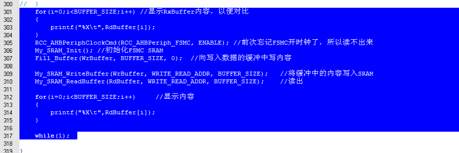
for(i=0;i<BUFFER_SIZE;i++) //显示RxBuffer内容,以便对比
{
printf("%X\t",RdBuffer[i]);
}
RCC_AHBPeriphClockCmd(RCC_AHBPeriph_FSMC, ENABLE); //前次忘记FSMC开时钟了,所以读不出来
My_SRAM_Init(); //初始化FSMC SRAM
Fill_Buffer(WrBuffer, BUFFER_SIZE, 0); //向写入数据的缓冲中写内容
My_SRAM_WriteBuffer(WrBuffer, WRITE_READ_ADDR, BUFFER_SIZE); //将缓冲中的内容写入SRAM
My_SRAM_ReadBuffer(RdBuffer, WRITE_READ_ADDR, BUFFER_SIZE); //读出
for(i=0;i<BUFFER_SIZE;i++) //显示内容
{
printf("%X\t",RdBuffer[i]);
}
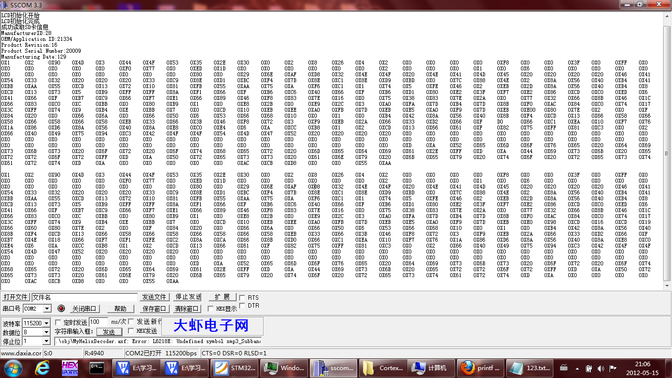
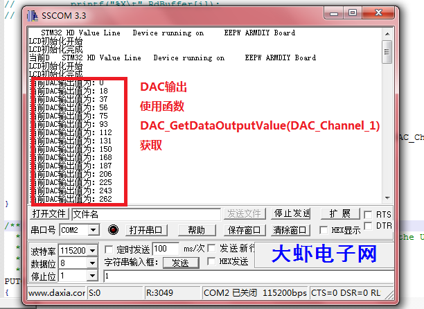
最后 上图:
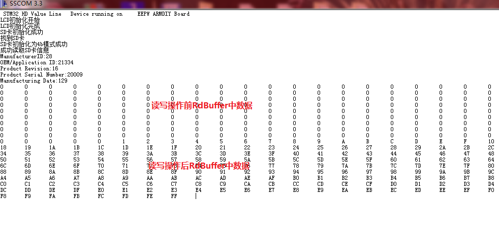
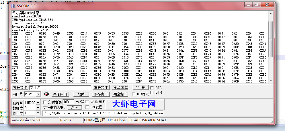
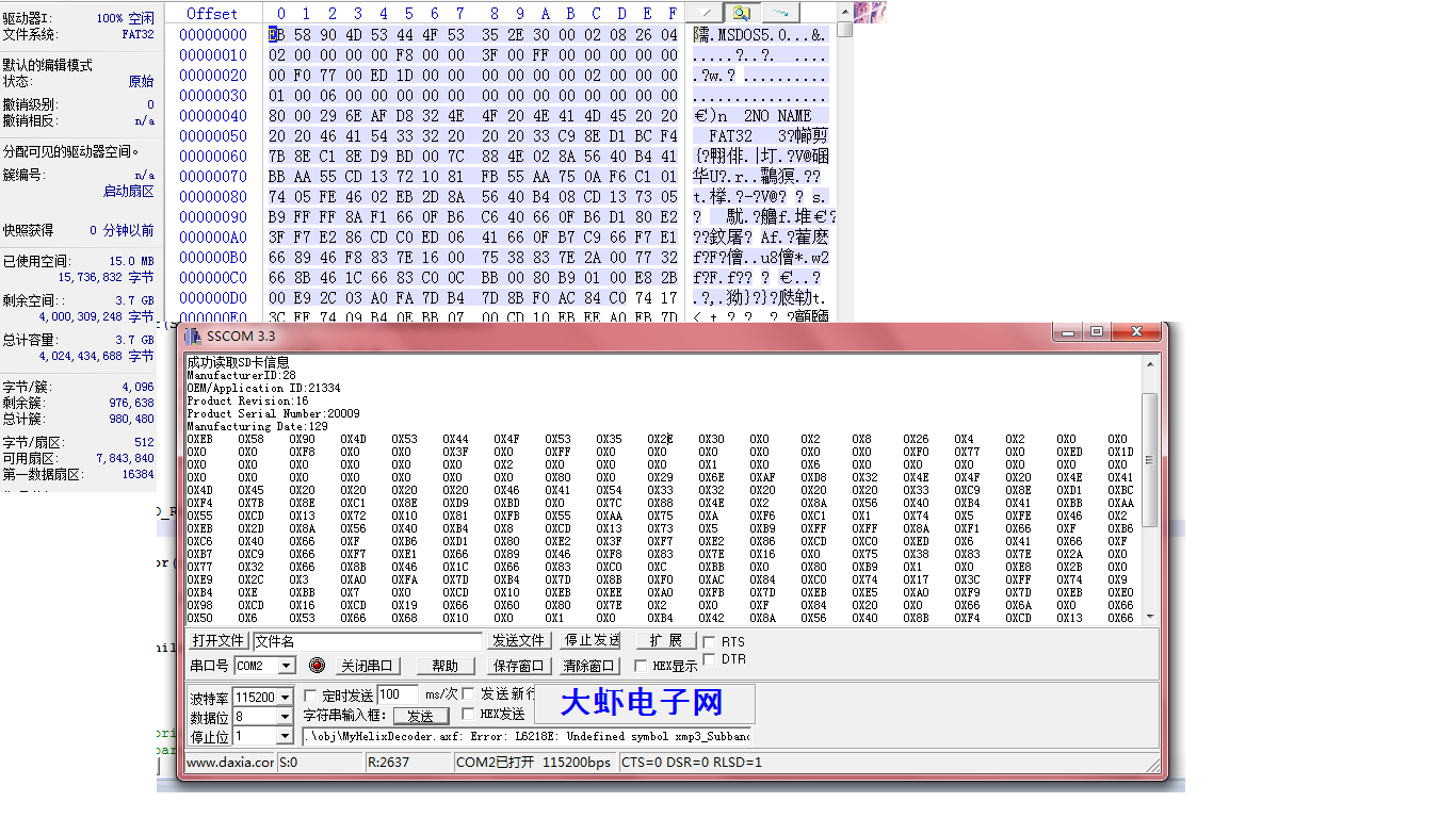
读SD卡数据到SRAM中,将SRAM当作个缓冲也不错哦。

 我要赚赏金
我要赚赏金 STM32
STM32 MCU
MCU 通讯及无线技术
 物联网技术
物联网技术 电子DIY
电子DIY 板卡试用
板卡试用 基础知识
基础知识 软件与操作系统
 我爱生活
我爱生活 小e食堂
小e食堂

