PCB layout design for switching power supply IC is as important as the circuit design. Appropriate layout can avoid various problems caused by power supply circuit. Major problems that arise from inappropriate layout may cause increase in noise superposed by output and switching signal, the deterioration of regulator, and also lack of stability. Adopting an appropriate layout will suppress these problems to occur.
Current Path
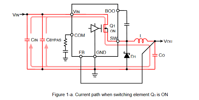
Figure 1-a to 1-c shows current path in a buck converter circuit. In Figure 1-a, the red line illustrates the main current flow in the converter when switching element Q1 is ON. CBYPASS is a decoupling capacitor for high frequency and CIN is the capacitor with large capacitance. The instance when the switching element Q1 is turned ON, most of the steep part of current waveform is supplied by CBYPASS and then from CIN.
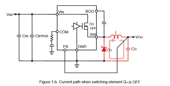
In Figure 1-b, the red line illustrates the condition of current flow when the switching element Q1 is OFF. Free-wheel diode D1turns ON and energy stored in inductor L gets released to output side. For Buck converter topology, since inductor is inserted at output in series the output capacitor current is smooth.
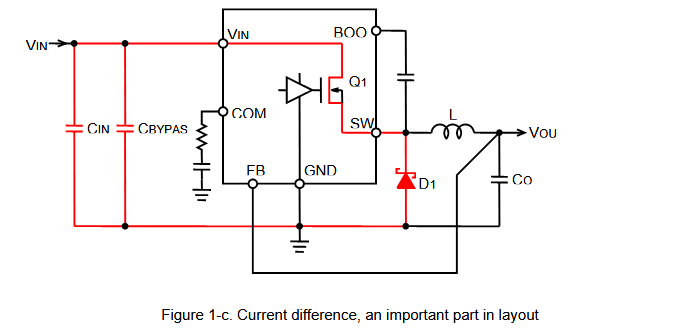
Refer Figure 1-c, the red line shows the difference between Figure 1-a and 1-b. Current in this red line changes violently each time the switching element Q1 changes from OFF to ON, and vice versa. These sharp changes induce several harmonics in the waveform. This difference in system needs to be paid maximum attention during PCB layout and an important caution point.
PCB Layout Procedure
General points of PCB layout procedure are as follows.
1. Place input capacitor and free-wheel diode on the same PCB surface layer as the IC terminal and as close as possible to IC.
2. Include thermal via if necessary to improve heat dissipation.
3. Place inductor close to IC, no need to be as close as input capacitor. This is to minimize radiation noise from the switching node and do not expand copper area more than needed.
4. Place output capacitor close to inductor.
5. Keep wiring of return path away from noise causing areas, such as inductor and diode.
Placing of input Capacitor and Free-wheel Diode
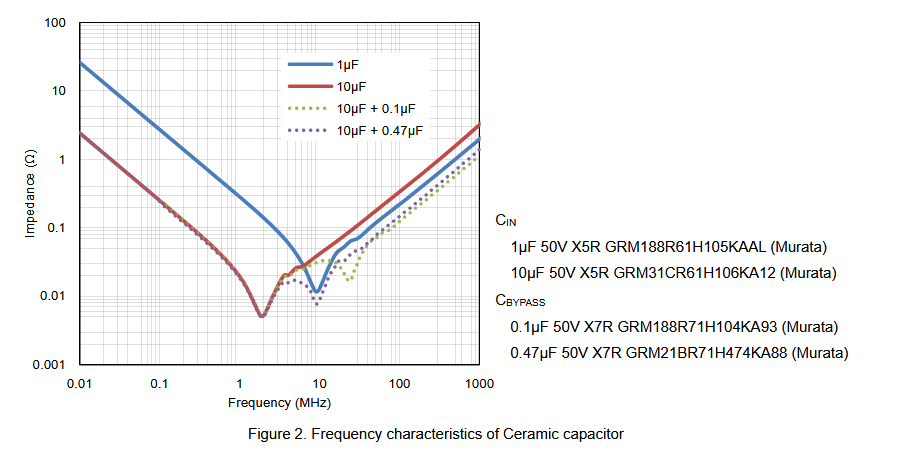
First of all, start placing the most important parts, such as the input capacitor and free-wheel diode. A Single ceramic capacitor may serve as both CIN and CBYPASS for smaller capacitance value of input capacitor, in designs with small current power supply (IO≤1A). This is because the frequency characteristics get better,as ceramic capacitor’s capacitance value gets smaller. But ceramic capacitor has different frequency characteristics, so confirming it for actual parts being used is important.
As in Figure 2, when a large capacitance value capacitor is used for CIN, generally it has bad frequency characteristics. Therefore place a decoupling capacitor CBYPASS for high frequency with good frequency characteristics in parallel to CIN. For CBYPASS, use surface mount type laminated ceramic capacitor with value of 0.1μF to 0.47μF, X5R or X7R type.
Figure 3-a shows layout example for a suitable input capacitor.Place CBYPASS near IC terminal on the top layer. As in Figure 3-b, large capacitance capacitor CIN can be separated about 2cm from CBYPASS that supplies most of the pulse-current. When difficulty in space occupied, and if cannot place CIN on the same surface as IC, it can be placed at the bottom layer through vialike in Figure 3-c. Risks regarding noise can be avoided with this, but there is a possibility of ripple-voltage to increase at high-current, influenced by via resistance.
Figure 3-d shows the layout of CBYPASS and CIN placed on the reverse side. In such case, voltage noise is created by inductance of the via, and the bypass capacitor operates as a reverse effect. Do not carry out this kind of layout design.


……未完待续……
点击此处,免费查看完整版“降压转换器的电路基板配置技巧”

 我要赚赏金
我要赚赏金

