
二极管和保护装置抑制瞬时高压静电放电。
在某些测量应用中,如pH值(酸度)和生物电势需要高阻抗缓冲放大器。虽然有几个半导体制造商提供具有低偏置和输入偏置电流特点的放大器芯片,配上传感器电缆可能会因为ESD(静电放电)对放大电路造成损害。图1显示一种不令人满意的方法实现ESD保护。电阻R1抑制ESD的放电电流,而二极管D1A 和D1B钳住放大器IC1的输入到供电电源轨。不幸的是,当并联pH值传感器的为400MΩ输入阻抗时,即使采用低漏电流二极管,如Fairchild公司的MMBD-1503A,仍引入很大的偏置电压。
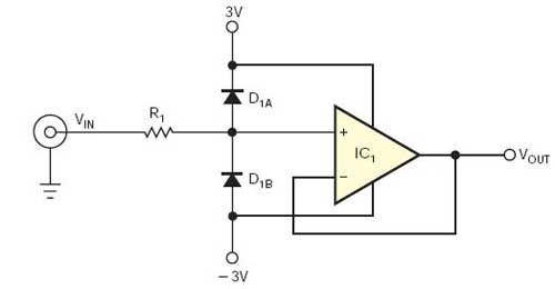
图2中的电路提供另一个方法。Analog Devices公司的低输入偏置,低偏置电流的AD8603放大器IC1,作为单位增益输入缓冲器。对于任何正常输入,电路的输出电压VOUT 等于其输入电压VIN。因此,电压经过ESD保护二极管D1A 和D1B接近0V,二极管漏电流均不影响传感器输出信号。依靠ESD适用电路输入连接器的极性,其高电压放电通过二极管D1A 或D1B进入供电正向或负向电源。电容C1充当中间“电荷存储器”,放慢ESD的上升速率,保护IC1的输出过程,从锁存到二极管D1A 或D1B开始分离ESD瞬流到正向或负向电源。实际上,C1补偿D1的寄生电容。电阻R3允许IC1来驱动电容负载,使C1不会进入振荡状态。
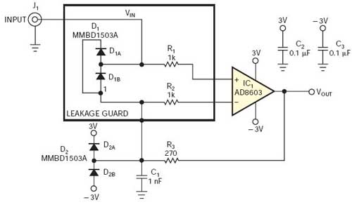
在ESD事件中,D1和D2可以进行传导,但通过两个前置偏移二极管压降,VIN端的电压超出供电电源电压。电阻R1和R2限制放大器输入电流在制造商建议的最大5mA之下。
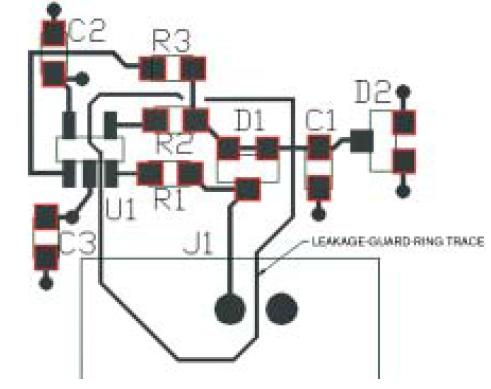
封装电路时,需要特别注意电路板的布局。电路板介电性能的缺陷会给寄生漏电流提供路径。在电路板的两面敷铜形成保护环,可以在电路高阻抗节点周围转移漏电流(图3)。
英文原文:
High-impedance buffer amplifier's input includes ESD protection
Diodes and guard traces suppress high-voltage static-discharge transients.
Certain measurement applications, such as for pH (acidity) and bio-potentials, require a high-impedance buffer amplifier. Although several semiconductor manufacturers offer amplifier ICs featuring low bias and offset-input currents, attaching a sensor cable to an amplifier circuit can inflict damage from ESD (electrostatic discharge). Figure 1 shows one unsatisfactory approach to ESD protection. Resistor R1 limits an ESD event's discharge current, and diodes D1A and D1B clamp amplifier IC1's input to its power-supply rails. Unfortunately, when shunting a pH sensor's 400-MΩ input impedance, even low-leakage diodes, such as Fairchild Semiconductor's MMBD-1503A, introduce significant offset voltages.
The circuit in Figure 2 offers an alternative approach. An Analog Devices low-input-bias, low-offset-current AD8603 amplifier, IC1, serves as a unity-gain input buffer. For any normal input, the circuit's output voltage, VOUT, equals its input voltage, VIN. Thus, the voltage across ESD-protection diode D1A or D1B approaches 0V, and neither diode's leakage current affects the sensor's output signal. Depending on the polarity of an ESD event you apply to the circuit's input connector, its high-voltage spike discharges through diode D1A or D1B into the positive or the negative power-supply rail. Capacitor C1 acts as an intermediate "charge reservoir" that slows the ESD spike's rate of rise and protects IC1's output stage from latching until diode D2A or D2B begins diversio
n of the ESD transient into the positive or the negative supply rail. In effect, C1 compensates for D1's parasitic capacitance. Resistor R3 allows IC1 to drive the capacitive load that C1 presents without going into oscillation.
During an ESD event, both D1 and D2 can conduct, but the voltage at VIN exceeds the power-supply-rail voltage by only two forward-biased diode voltage drops. Resistors R1 and R2 limit the amplifier input's currents below the manufacturer's recommended 5-mA maximum rating.
When packaging the circuit, pay special attention to the pc board's layout. Imperfections in the board's dielectric properties can provide parasitic-leakage-current paths. Adding copper traces on both sides of the board to form guard rings around the circuit's high-impedance nodes diverts leakage currents (Figure 3).
 我要赚赏金
我要赚赏金 STM32
STM32 MCU
MCU 通讯及无线技术
 物联网技术
物联网技术 电子DIY
电子DIY 板卡试用
板卡试用 基础知识
基础知识 软件与操作系统
 我爱生活
我爱生活 小e食堂
小e食堂

